Method for producing protein chip

A protein chip and manufacturing method technology, applied in the field of biosensing, can solve the problem of low integration and achieve the effect of ensuring activity

Inactive Publication Date: 2004-09-15
SHANGHAI UNIV
View PDF0 Cites 3 Cited by
  • Summary
  • Abstract
  • Description
  • Claims
  • Application Information

AI Technical Summary

Problems solved by technology

Traditional photolithography technology, the minimum size of the pattern etched on the silicon surface can only reach a few hundred nanometers to a few microns, and its integration level is not high, and it needs to be further improved by 1 to 2 orders of magnitude to meet the requirements of today's technology. on request

Method used


Image

  • Method for producing protein chip

Examples


Embodiment 1

[0016] Embodiment 1: the concrete processing steps of the present invention are as follows:

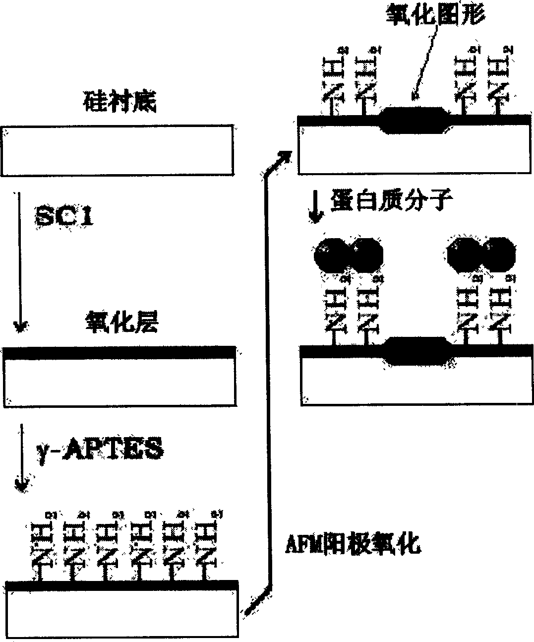
[0017] a. First, standard semiconductor technology is used to clean and thermally oxidize the silicon wafer; the surface of the cleaned and thermally oxidized silicon wafer has a layer of 500 nanometer silicon dioxide layer;

[0018] b. immerse the above-mentioned pretreated silicon wafer in γ-amino-propyl-triethylsilane (γ-APTES) for 10 minutes, so that the surface of the silicon wafer has amino groups and has affinity for protein molecules;

[0019] c. Adopt atomic force microscope (AFM) nano-etching technology to etch nano-patterns on the above-mentioned processed silicon wafer surface; the etching method is: apply a voltage between the atomic force microscope probe and the silicon surface, so that Atoms are oxidized into silicon dioxide; the probe is moved and etched into a square array with a side length of 200 nanometers and a line width of 50 nanometers. The amino group on the ...

Embodiment 2

[0021] Embodiment two: the concrete processing steps of the present invention are as follows:

[0022] a. First, standard semiconductor technology is used to clean and thermally oxidize the silicon wafer; there is a silicon dioxide layer of 800 nanometers on the surface of the cleaned and thermally oxidized silicon wafer;

[0023] b. immerse the above-mentioned pretreated silicon wafer in γ-amino-propyl-triethylsilane (γ-APTES) for 10 minutes, so that the surface of the silicon wafer has amino groups and has affinity for protein molecules;

[0024] c. Adopt atomic force microscope (AFM) nano-etching technology to etch nano-patterns on the above-mentioned processed silicon wafer surface; the etching method is: apply a voltage between the atomic force microscope probe and the silicon surface, so that Atoms are oxidized into silicon dioxide; move the probe, etch concentric circles with a radius of 200 nanometers and 400 nanometers and a line width of 50 nanometers. The 100 nm an...


PUM


Abstract

Substantially, the invention is a method for fixing active protein molecules on surface of silicon, applicable to preparation of DNA chip and protein chip, belonging to area of biologic sensing technique. Characters of the invention are as follows. First, standard semiconductor technology is utilized to clean and oxidate silicon slice in high temperature. Next, silicon surface is treated by using gamma - amido - propyl - triethyl silane (gamma-APTES). Then, graph in nano size is etched on silicon surface by using nano etching technique of atomic force microscope (ATM). Finally, the silicon slice with prepared Nano graph is immersed into solution of protein. Thus, protein molecules are fixed on not etched silicon surface, and there is no protein molecule on the etched silicon surface. Advantages of the invention are: ensuring active of protein molecules effectively, and superhigh integration level of protein molecules.

Description

technical field [0001] The invention relates to a method for manufacturing a protein chip, which is essentially a method for immobilizing active protein molecules on a silicon surface. The method can be applied to the manufacture of DNA chips and protein chips, and belongs to the technical field of biosensing. Background technique [0002] A DNA chip or a protein chip integrates a variety of DNA or protein activities on a very small geometric surface area. With only a small amount of biological (physiological) sampling, different molecules, including the interaction between molecules and gene expression, can be detected and studied at the same time, and the conditional changes of molecular groups under various conditions can be obtained, so that the laws of life activities can be obtained. Biomolecular chips and biomolecular recognition and detection technology have now become the frontier technology of biomedical engineering in the 21st century. [0003] As we all know, be...

Claims


Application Information

Patent Timeline
Patent Type & Authority Applications(China)
IPC IPC(8): C12Q1/68G01N33/50G01N33/543G01N33/68
Inventor 焦正吴明红施利毅金丽娟
Owner SHANGHAI UNIV
Why Eureka
Try Eureka