Method for forming dielectric film in trenches by PEALD using H-containing gas

a dielectric film and trench technology, applied in the direction of basic electric elements, semiconductor/solid-state device manufacturing, electric apparatus, etc., can solve the problems of insufficient resolution of the different etch rate between the sidewall and the top surface, and the thickness of the film deposited on the sidewall of the trench is relatively high, so as to increase the deposition rate of film. , the effect of increasing the thickness of the film

Active Publication Date: 2016-09-27
ASM IP HLDG BV
View PDF1347 Cites 397 Cited by
  • Summary
  • Abstract
  • Description
  • Claims
  • Application Information

AI Technical Summary

Benefits of technology

[0007]In some embodiments of the present invention, the thickness of film deposited on a target side of a trench of semiconductor circuits (substrate) can be controlled. In some embodiments, the thickness of film deposited on a sidewall of a trench relatively increases, i.e., the thickness of film deposited on a top (blanket) surface of the substrate relatively decreases. In one approach, the thickness of film on a sidewall of a trench can be controlled by controlling chemisorption of a precursor on a surface using a chemisorption-inhibitor gas to which the substrate is exposed as a preliminary treatment before depositing a film thereon, wherein functional groups exposed on the top surface of the substrate are terminated by Si—H bonds using a chemisorption-inhibitor gas such as hydrogen gas, thereby interfering with chemisorption of the precursor on the top surface and relatively increasing the deposition rate of film on the sidewall. In some embodiments of the present invention, another approach other than the above approach is taken, wherein when depositing a silicon-based dielectric film such as a SiC or SiN film by PEALD, a hydrogen-containing gas is used as a reactant gas so as to cause not only deposition of a film but also etching of the film by a plasma. Since more species excited by a plasma reach a flat surface, i.e., a top surface of a substrate and a bottom of a trench of the substrate, than excited species reaching a sidewall of the substrate, by controlling process parameters including feed quantity of a precursor and intensity and duration of a hydrogen plasma, controlling and balancing deposition and etching of film can be accomplished predominantly on a flat surface, whereby the thickness of film at the sidewall of the trench can be adjusted relative to the thickness of film on the flat surface of the substrate (the sidewall receives less effect of a plasma than does the flat surface). In the above, a film is being deposited by excited species of precursor while being etched by hydrogen and argon plasma, for example.

Problems solved by technology

However, in plasma-enhanced atomic layer deposition (PEALD), since a sidewall of a trench of a substrate undergoes less ion bombardment than does a top surface of the substrate, surface reaction at the sidewall is less active than on the top surface, causing a problem that an etch rate of a film at the sidewall is different from (higher than) that on the top surface.
However, the improvement is partial, and the problem in different etch rates between the sidewall and the top surface is not sufficiently resolved.

Method used


Image

  • Method for forming dielectric film in trenches by PEALD using H-containing gas
  • Method for forming dielectric film in trenches by PEALD using H-containing gas
  • Method for forming dielectric film in trenches by PEALD using H-containing gas

Examples


examples

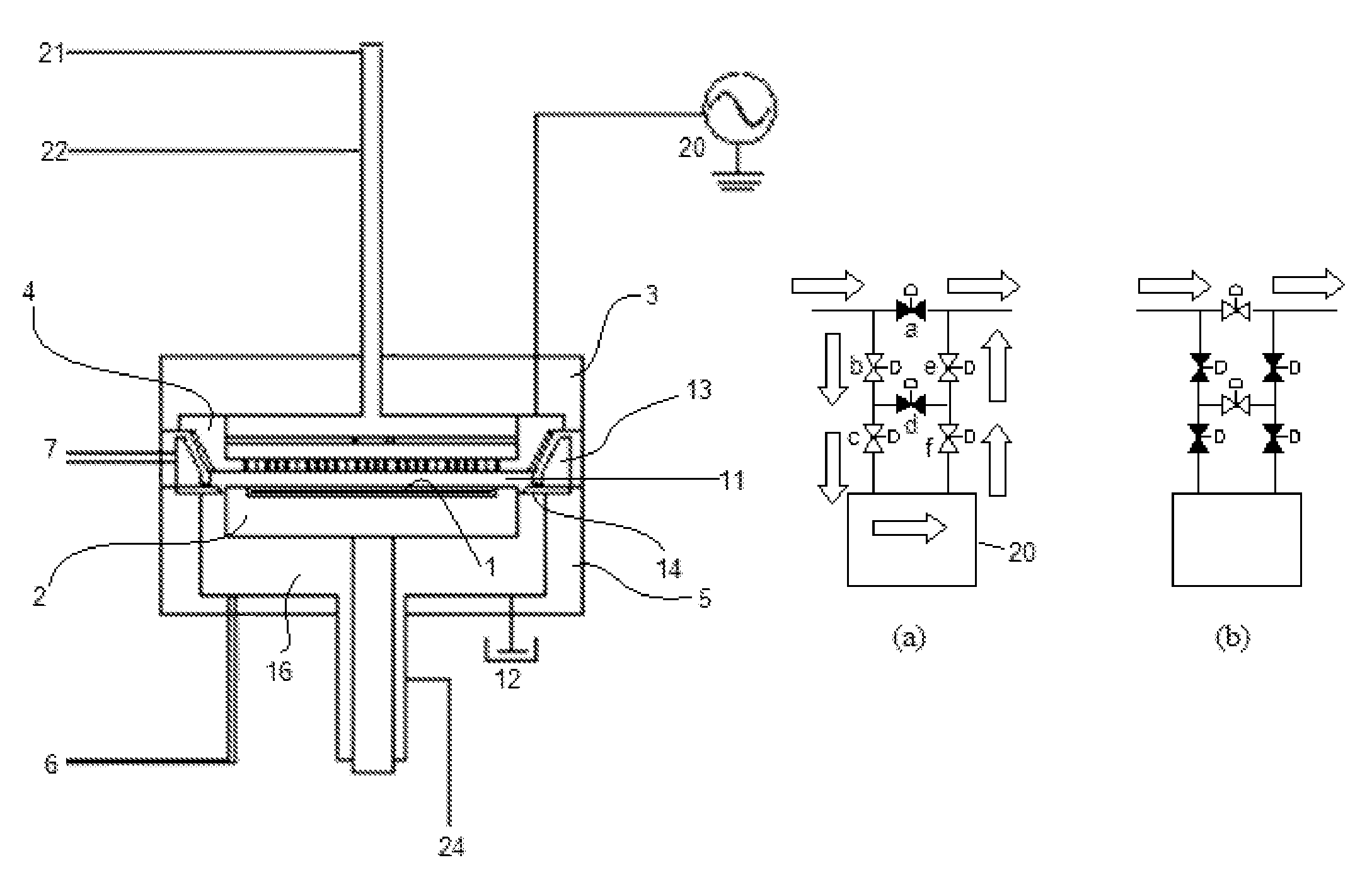
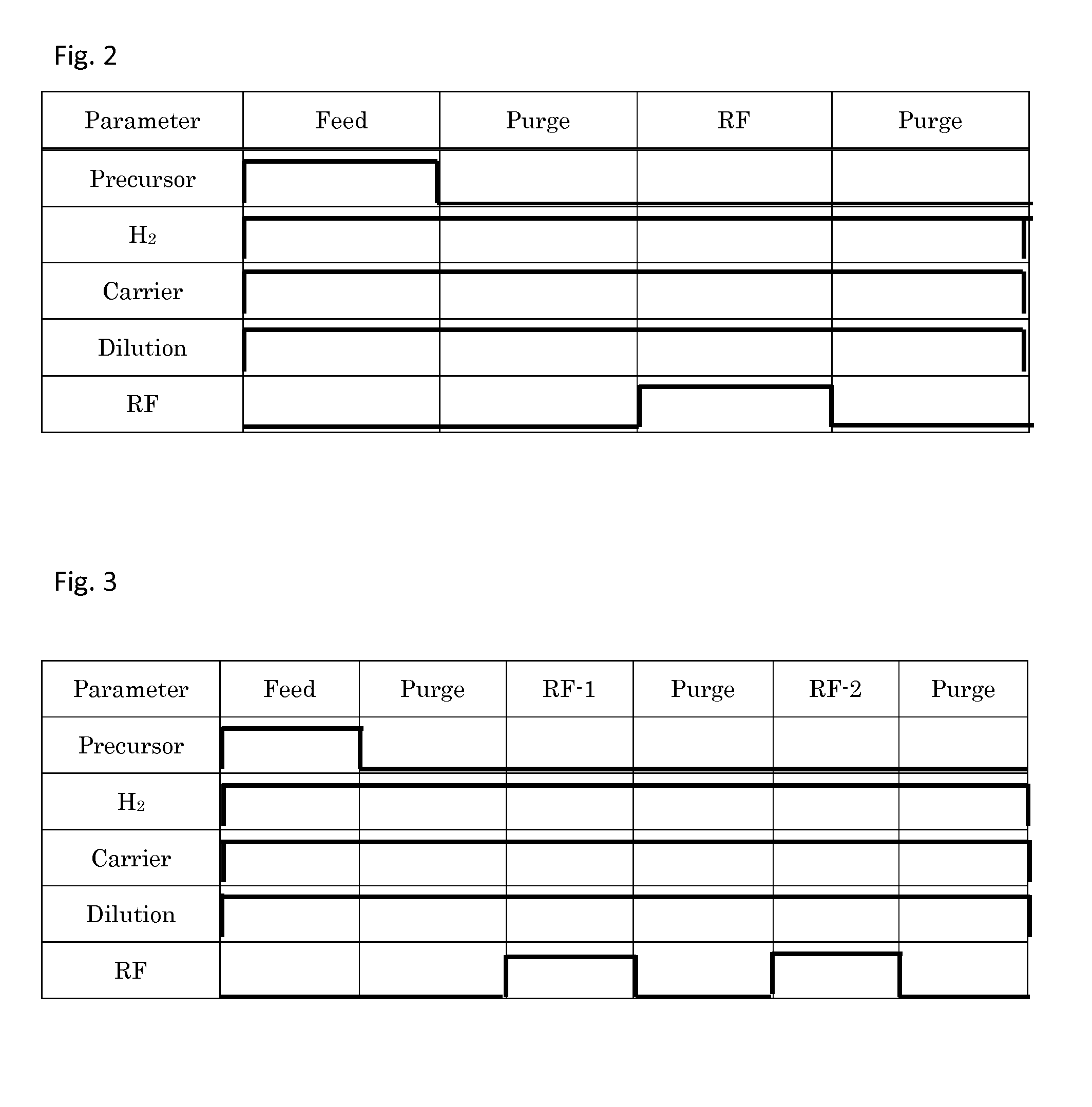
[0051]A silicon carbide film was formed on a Si substrate (0300 mm) having trenches with an aspect ratio of 3.5 (a width of 30 nm, and a depth of 110 nm) by PEALD using a sequence illustrated in FIG. 2 or 3, one cycle of which was conducted under the common conditions shown in Table 2 (process cycle) below using the PEALD apparatus illustrated in FIG. 1A and a gas supply system (FPS) illustrated in FIG. 2 with the specific conditions and sequence indicated in Table 3.

[0052]

TABLE 2(the numbers are approximate)Common Conditions for Process CycleSubstrate temperature300.° C.Pressure300 PaCarrier gas and dilution gasArReactant gasH2Flow rate of carrier / dilution gas 2000 sccm / 1000 sccm (continuous)(3000 sccm total)Purge after precursor feed pulse1 secPurge after RF power pulse1 secRF power100 WTarget Thickness (nm)10.

[0053]

TABLE 3(the numbers are approximate)Feed RF H2 FeedamountpulseflowSequence(seconds)(g / cycle)(seconds)Precursor(sccm)*1FIG. 210.041DVDMS0*2FIG. 20.10.0041DVDMS800*3FIG....


PUM


Abstract

A method for forming a dielectric film in a trench on a substrate by plasma-enhanced atomic layer deposition (PEALD) performs one or more process cycles, each process cycle including: (i) feeding a silicon-containing precursor in a pulse; (ii) supplying a hydrogen-containing reactant gas at a flow rate of more than about 30 sccm but less than about 800 sccm in the absence of nitrogen-containing gas; (iii) supplying a noble gas to the reaction space; and (iv) applying RF power in the presence of the reactant gas and the noble gas and in the absence of any precursor in the reaction space, to form a monolayer constituting a dielectric film on a substrate at a growth rate of less than one atomic layer thickness per cycle.

Description

BACKGROUND[0001]1. Field of the Invention[0002]The present invention generally relates to a method for depositing a dielectric film in a trench of a substrate by plasma-enhanced atomic layer deposition (PEALD). The present invention also relates to a method for increasing a sidewall coverage of a dielectric film deposited by PEALD.[0003]2. Related Art[0004]As a method of depositing a film having a good step coverage, atomic layer deposition (ALD) using chemisorption of a precursor is commonly performed. In this method, a film deposits more evenly in trenches of semiconductor circuits than does a film by CVD or the like. However, in plasma-enhanced atomic layer deposition (PEALD), since a sidewall of a trench of a substrate undergoes less ion bombardment than does a top surface of the substrate, surface reaction at the sidewall is less active than on the top surface, causing a problem that an etch rate of a film at the sidewall is different from (higher than) that on the top surface....

Claims


Application Information

Patent Timeline
Patent Type & Authority Patents(United States)
IPC IPC(8): H01L21/311H01L21/02
CPCH01L21/0228H01L21/02208H01L21/02123H01L21/02211H01L21/02274
Inventor FUKAZAWA, ATSUKIFUKUDA, HIDEAKITAKAMURE, NOBORUZAITSU, MASARU
Owner ASM IP HLDG BV
Why Eureka
Try Eureka