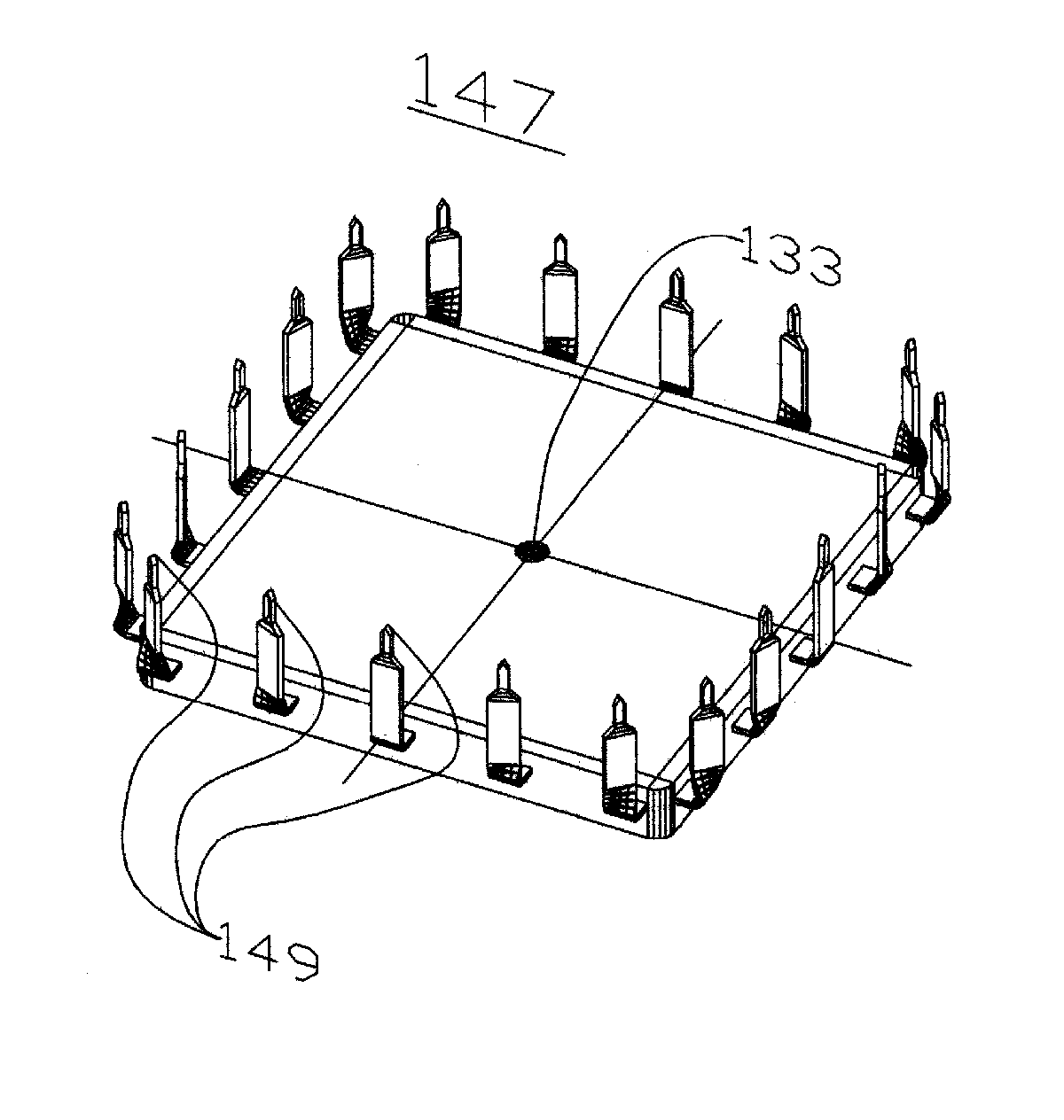
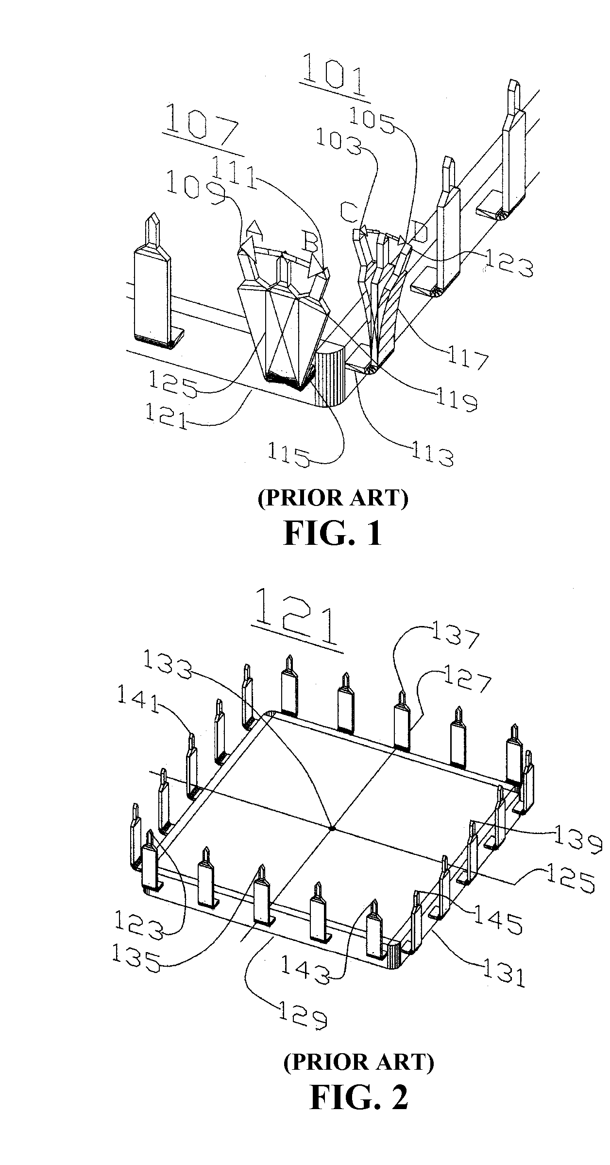
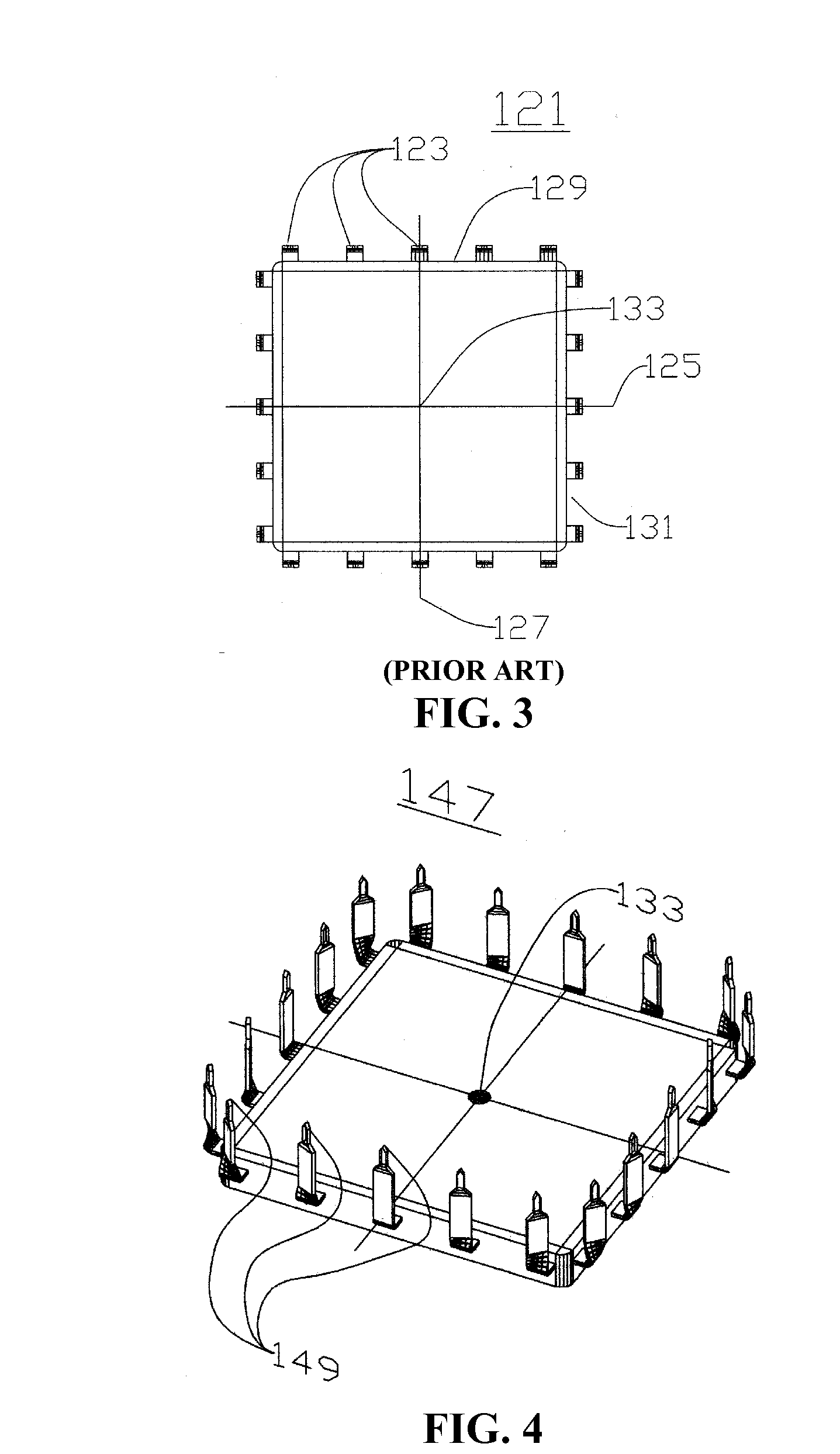
No-wick(TM) 2 interconnections

Inactive Publication Date: 2007-12-13
CHERIAN GABE
View PDF4 Cites 18 Cited by
  • Summary
  • Abstract
  • Description
  • Claims
  • Application Information

AI Technical Summary

Benefits of technology

[0079] The main goal and the advantage of the proposed changes and improvements are to make the leads more flexible, thus requiring less force to hold them in place at their anchor points in the body of the package. This translate itself into a situation, where the encapsulating plastic of the body, at the anchor or base of the leads, would be less stressed, thus less apt to crack or to generate those undesirable micro-cracks, which in turn would mean that the moisture would have less chance to penetrate to the insides of the package, thus prolonging the life of the chip and the package. In short, this translates into improving the reliability of the package. A corollary resulting advantage is that the interconnections between the package and the substrates would last longer and the whole system would be more reliable.

Problems solved by technology

The Cherian Solder Columns, however, cannot readily be simply scaled down to the new center distances required by present components.
The old inventions can no longer keep up with such miniaturization
It will take too many pages.

Method used


Image

  • No-wick(TM) 2 interconnections
  • No-wick(TM) 2 interconnections
  • No-wick(TM) 2 interconnections

Examples


first embodiment

[0360]FIG. 43 shows a first embodiment as per this invention. It is a column with solder control dam.

[0361]FIGS. 44 through 49 show applications of this embodiment.

second embodiment

[0362]FIG. 50 shows a It is “treated” column.

[0363]FIGS. 51 through 56 show applications of this second embodiment.

[0364]FIG. 57 shows a “carrying wafer”, which can be used to handle a number of columns as per this invention. It also shows an “anchor”.

[0365]FIG. 58 shows several methods of implementing the teaching of the invention.

[0366]FIGS. 59 and 60 show some fixturing used in implementing the invention

[0367]FIG. 61 shows how “wire bonding” can be used to implement the invention.

[0368]FIGS. 62 and 63 show details of wire bonded columns and how to mount chips or packages on substrates or boards, using wire bonded columns.

[0369]FIGS. 64 through 68 show details of how to coat the wire bonded columns to prepare them as solder controlled columns.

[0370]FIG. 69 shows details of solder joints in recesses in the solder resist coating.

[0371]FIG. 70 shows a concept of a machine that can be used to wire bond discrete pieces of wire.

[0372]FIG. 71 shows a chip on a substrate, or a p...


PUM


Abstract

The present invention relates generally to permanent interconnections between electronic devices, such as integrated circuit packages, chips, wafers and printed circuit boards or substrates, or similar electronic devices. More particularly it relates to high-density electronic devices. The invention describes means and methods that can be used to counteract the undesirable effects of thermal cycling, shock and vibrations and severe environment conditions in general. For leaded devices, the leads are oriented to face the thermal center of the devices and the system they interact with. For leadless devices, the mounting elements are treated or prepared to control the migration of solder along the length of the elements, to ensure that those elements retain their desired flexibility.

Description

CROSS-REFERENCE TO RELATED APPLICATIONS [0001] This application is a DIVISIONAL UTILITY PATENT APPLICATION, BASED ON patent application Ser. No. 10 / 937,647, ENTITLED “INTERCONNECTIONS”, which was filed on Sep. 8, 2004, which in turn is a DIVISIONAL UTILITY PATENT APPLICATION, BASED ON patent application Ser. No. 10 / 075,060, ENTITLED “INTERCONNECTIONS”, which was filed on Mar. 17, 2003, the latter having been granted the U.S. Pat. No. 6,884,707 B1, issued Apr. 26, 2005. [0002] This application is claiming the priority and benefits of the same references, which were claimed by the two mother applications. These references are the following six patent applications, which are three provisional patent applications and two non-provisional utility patent applications, all of which are incorporated herein in their entirety by reference: [0003] 1) Provisional Patent Application Ser. No. 60 / 231,387, filed Sep. 8, 2000, entitled “Probers”, which will be referred to as Ref1, and [0004] 2) Provi...

Claims


Application Information

Patent Timeline
IPC IPC(8): H01L23/495
CPCH01L21/4853H01L21/6835H01L23/49555H01L23/49811H01L24/11H01L24/12H01L24/16H01L24/48H01L24/72H01L24/73H01L24/742H01L24/85H01L2224/0401H01L2224/0603H01L2224/1134H01L2224/1308H01L2224/13083H01L2224/13124H01L2224/13147H01L2224/13184H01L2224/13582H01L2224/136H01L2224/13655H01L2224/1403H01L2224/16H01L2224/4556H01L2224/45599H01L2224/48247H01L2224/49171H01L2924/01002H01L2924/01004H01L2924/01011H01L2924/01013H01L2924/01014H01L2924/01015H01L2924/01027H01L2924/01029H01L2924/01047H01L2924/01057H01L2924/01074H01L2924/01075H01L2924/01078H01L2924/01079H01L2924/01082H01L2924/01322H01L2924/09701H01L2924/14H01L2924/15312H01L2924/15331H01L2924/19041H01L2924/3025H05K3/308H05K3/3426H05K2201/09418H05K2201/10318H05K2201/10424H05K2201/10689H05K2201/10704H05K2201/10719H05K2201/10734H05K2201/10825H05K2201/10871H05K2201/10946H05K2201/10977H05K2203/0769H01L2224/1601H01L24/49H01L2924/00013H01L2924/01005H01L2924/01006H01L2924/01019H01L2924/01023H01L2924/01033H01L2924/01043H01L2924/014H01L2224/85H01L2224/45147H01L2924/3511H01L2224/11822H01L2924/01028H01L2924/10253H01L2924/15747H01L2224/16225H01L2224/73257H01L2924/15311H01L2224/11334H01L2224/16235H01L2924/00014H01L2224/13099H01L2924/00H01L2224/29099H01L2224/45124H01L2924/181H01L24/45H01L24/13H01L2224/1012H01L2224/73203H01L2224/81903H01L2224/73251Y02P70/50H01L2924/00012H01L2224/05599H01L2224/72
Inventor CHERIAN, GABE
Owner CHERIAN GABE
Why Eureka
Try Eureka