Semiconductor integrated circuit device
- Summary
- Abstract
- Description
- Claims
- Application Information
AI Technical Summary
Benefits of technology
Problems solved by technology
Method used
Image
Examples
first example
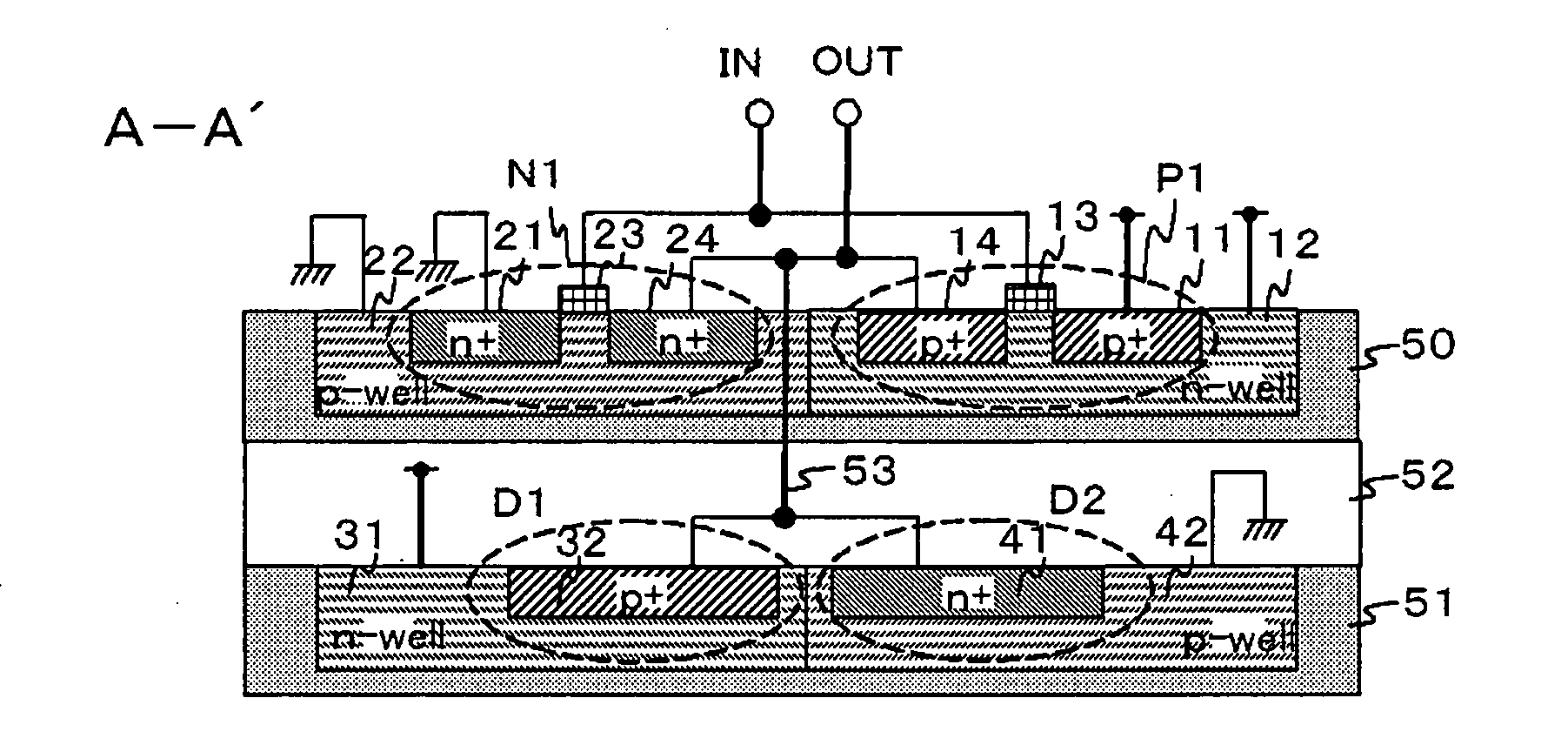
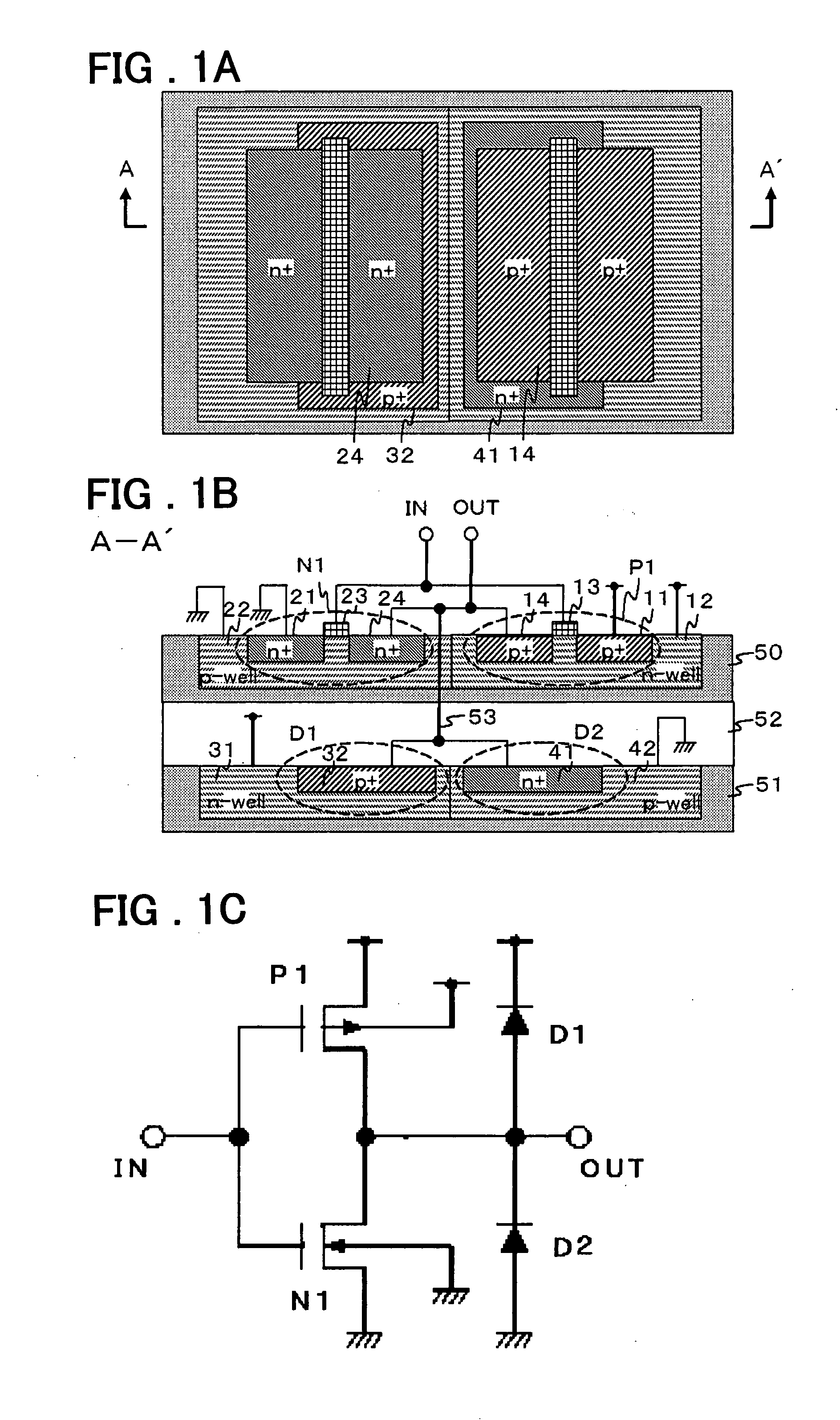
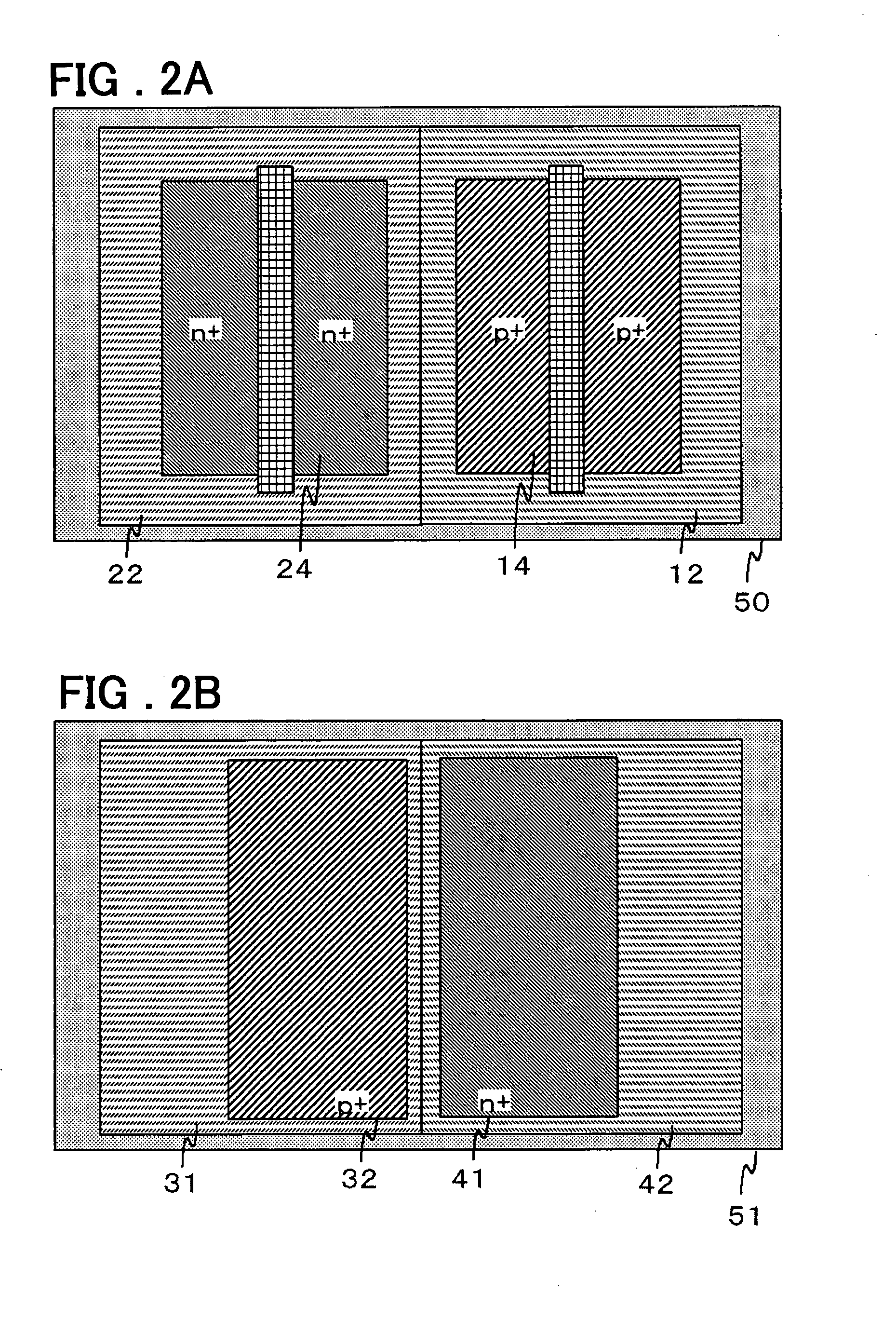
[0037]FIG. 1 includes diagrams showing a structure and a circuit of a semiconductor integrated circuit device according to a first example of the present invention. FIG. 1A is a plan view of the semiconductor integrated circuit device. FIG. 1B is a sectional view taken along a line A-A′ of the semiconductor integrated circuit device shown in FIG. 1A. FIG. 1C is a circuit diagram of the semiconductor integrated circuit device. Referring to FIGS. 1A, 1B and IC, the semiconductor integrated circuit device is an inverter circuit of the CMOS type, and includes a P-channel transistor P1, an N-channel transistor N1, and diodes D1 and D2. A source (a P+ diffusion layer 11) and a back gate (an n well 12) of the P-channel transistor P1 are connected to the power supply. A gate 13 of the P-channel transistor P1 is connected to an input terminal IN, and a drain (a p+ diffusion layer 14) of the P-channel transistor P1 is connected to an output terminal OUT. A source (an n+ diffusion layer 21) an...
second example
[0049]FIG. 6 is a circuit diagram of a semiconductor integrated circuit device according to a second example of the present invention. A logic circuit shown in FIG. 6 is a two-input NOR circuit of the CMOS type, and includes a P-channel transistor P2 and a P-channel transistor P3, an N-channel transistor N2 and an N-channel transistor N3, and the diodes D1 and D2. A source and a back gate of the P-channel transistor P2 is connected to the power supply, a gate of the P-channel transistor P2 is connected to an input terminal IN1, and a drain of the P-channel transistor P2 is connected to a source of the P-channel transistor P3. A back gate of the P-channel transistor P3 is connected to the power supply. A gate of the P-channel transistor P3 is connected to an input terminal IN2. A drain of the P-channel transistor P3 is connected to the output terminal OUT. A source and a back gate of each of the N-channel transistor N2 and the N-channel transistor N3 are grounded. A gate of the N-cha...
third example
[0053]FIG. 7 is a circuit diagram of a semiconductor integrated circuit device according to a third example of the present invention. A logic circuit shown in FIG. 7 is a two-input NAND circuit of the CMOS type, and includes a P-channel transistor P4 and a P-channel transistor P5, an N-channel transistor N4 and an N-channel transistor N5, and the diodes D1 and D2. A source and a back gate of each of the P-channel transistor P4 and the P-channel transistor P5 are connected to the power supply. A gate of the P-channel transistor P4 is connected to an input terminal IN3, and a gate of the P-channel transistor P5 is connected to an input terminal IN4. A drain of each of the P-channel transistor P4 and the P-channel transistor P5 is connected to the output terminal OUT. A source of the N-channel transistor N4 is connected to a drain of the N-channel transistor N5. A gate of the N-channel transistor N4 is connected to the input terminal IN3. A back gate of the N-channel transistor N4 is g...
PUM
 Abstract
Description
Claims
Application Information


