
Common-mode filter

Active Publication Date: 2007-12-13
TDK CORPARATION
View PDF5 Cites 15 Cited by
  • Summary
  • Abstract
  • Description
  • Claims
  • Application Information

AI Technical Summary

Benefits of technology

[0006] Therefore, the input and output portions of the respective coils are located close to each other through a layer, thereby increasing stray capacitance. As a result, the resonance frequency decreases, thereby lowering the common-mode characteristic in a high-frequency band. Further, since the individual portions of the coil are adjacent to each other on the same layer, the electric strength between coil lines may decrease.
[0019] The present invention can provide a common-mode filter which can simplify its manufacturing step without causing problems such as those of stray capacitance and electric strength between lines.

Problems solved by technology

Further, since the individual portions of the coil are adjacent to each other on the same layer, the electric strength between coil lines may decrease.
However, manufacturing such a multilayer common-mode filter increases processes, thereby complicating the manufacturing step, which becomes another problem to overcome.

Method used


Image

  • Common-mode filter
  • Common-mode filter
  • Common-mode filter

Examples


first embodiment

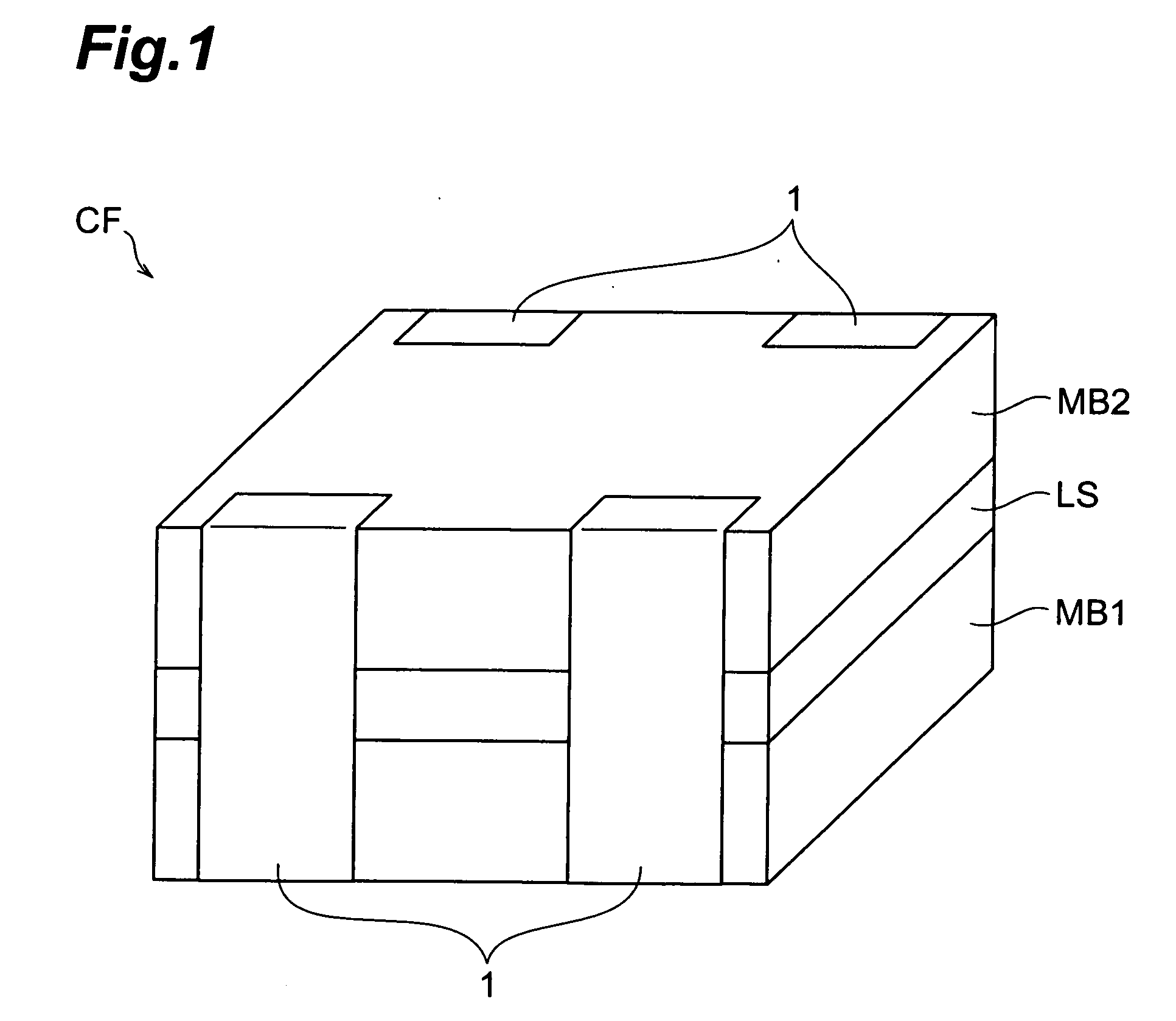
[0032] A common-mode filter which is a first embodiment will be explained with reference to FIG. 1. FIG. 1 is a perspective view showing a common-mode filter CF.

[0033] As shown in FIG. 1, the common-mode filter CF is a common-mode filter of a thin film type comprising a first magnetic substrate MB1, a layer structure LS, and a second magnetic substrate MB2. Terminal electrodes 1 are formed on the outer peripheral face of the multilayer body constructed by the first magnetic substrate MB1, layer structure LS, and second magnetic substrate MB2. The terminal electrodes 1 are formed such as to extend from the first magnetic substrate MB1 to the second magnetic substrate MB2 by way of the layer structure LS. The terminal electrodes 1 are formed by two pairs on two opposing side faces of the above-mentioned multilayer body.

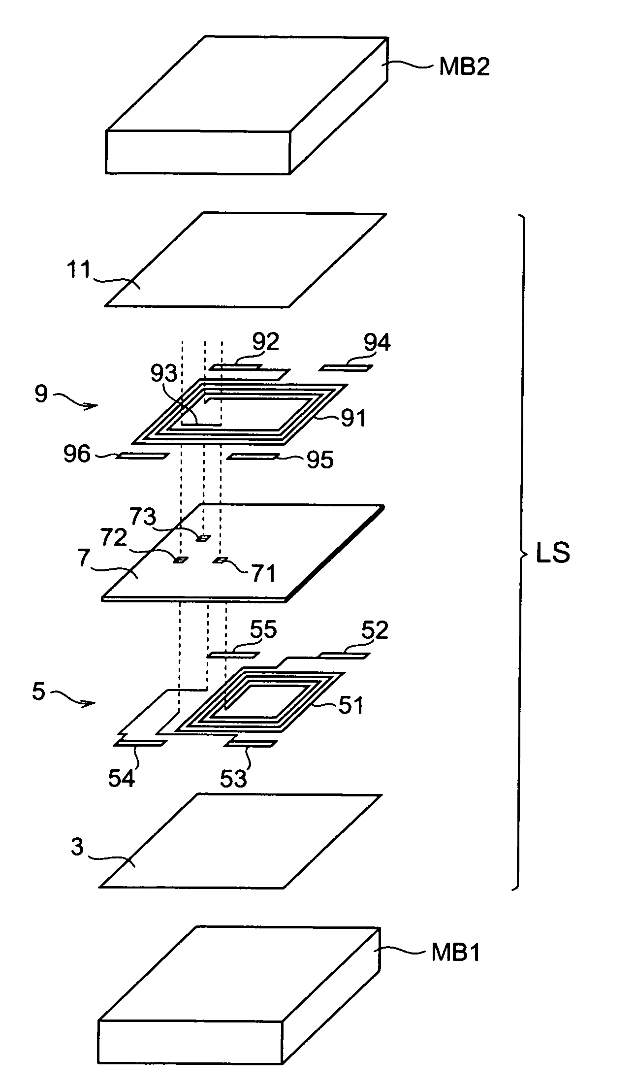
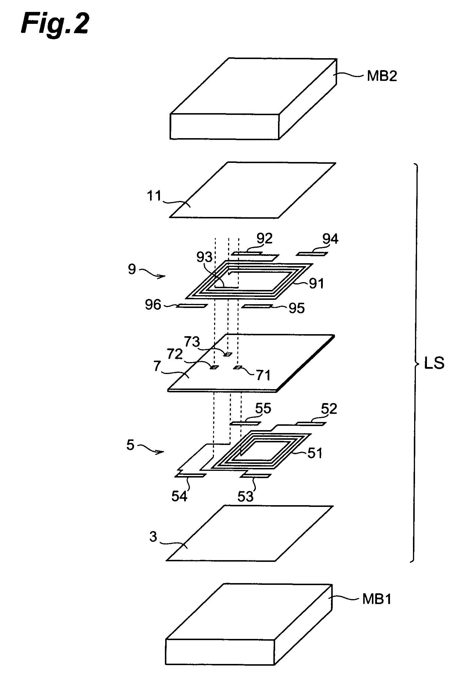
[0034]FIG. 2 is a schematic view showing the common-mode filter CF in an exploded fashion. The layer structure LS will be explained with reference to FIG. 2. As shown...

second embodiment

[0065] A common-mode filter which is a second embodiment of the present invention will be explained with reference to FIG. 4. FIG. 4 is a perspective view showing a common-mode filter CF2.

[0066] As shown in FIG. 4, the common-mode filter CF2 is a common-mode filter of a thin film type comprising a first magnetic substrate MB3, a layer structure LS2, and a second magnetic substrate MB4. Terminal electrodes 2 are formed on the outer peripheral face of the multilayer body constructed by the first magnetic substrate MB3, layer structure LS2, and second magnetic substrate M4. The terminal electrodes 2 are formed such as to extend from the first magnetic substrate MB3 to the second magnetic substrate MB4 by way of the layer structure LS2. The terminal electrodes 2 are formed by four pairs on two opposing side faces of the above-mentioned multilayer body.

[0067]FIG. 5 is a schematic view showing the common-mode filter CF2 in an exploded fashion. The layer structure LS2 will be explained w...

third embodiment

[0125] A common-mode filter which is a third embodiment of the present invention will be explained with reference to FIG. 8. The common-mode filter of this embodiment is provided with a first conductor layer 205, a second insulating layer 207, and a second conductor layer 209, which are shown in FIG. 8, in place of the first conductor layer 5, second insulating layer 7, and second conductor layer 9 in the common-mode filter CF of the first embodiment.

[0126] The first conductor layer 205 is formed on the first insulating layer 3 (see FIG. 2). As shown in (a) in FIG. 8, the first conductor layer 205 has a spiral part (second spiral part) 251, a lead electrode 252, a lead electrode 253 (second lead electrode), a lead electrode 254, a lead electrode 255, and a connecting conductor 256. The lead electrodes 252, 253 are arranged on one side of the first insulating layer 3, whereas the lead electrodes 254, 255 are arranged on one side of the first insulating layer 3 opposing the side ther...


PUM


Abstract

A common-mode filter comprises a first conductor layer, a second conductor layer, and an insulating layer placed between the first and second conductor layers. The first conductor layer has a first spiral part formed such as to draw a convolution and a first lead electrode extending from one end of the first spiral part. The second conductor layer has a second spiral part formed such as to draw a convolution and a second lead electrode extending from one end of the second spiral part. The first conductor layer is formed with third and fourth lead electrodes. The second conductor layer is formed with a connecting conductor connecting the third lead electrode to the other end of the first spiral part. The fourth lead electrode is connected to the other end of the second spiral part through a contact hole formed in the insulating layer. The third lead electrode is connected to one end of the connecting conductor through a contact hole formed in the insulating layer. The other end of the connecting conductor is connected to the other end of the first spiral part through a contact hole formed in the insulating layer.

Description

BACKGROUND OF THE INVENTION [0001] 1. Field of the Invention [0002] The present invention relates to a common-mode filter. [0003] 2. Related Background Art [0004] As electronic devices such as personal computers and cellular phones have been becoming smaller, electronic components such as coils and capacitors mounted in inner circuits of the electronic devices have been demanded to be made smaller and thinner. Known as one of thin-film coil components responding to such a demand is a common-mode filter (see, for example, Japanese Patent Application Laid-Open No. 2005-50957). SUMMARY OF THE INVENTION [0005] The common-mode filter disclosed in Japanese Patent Application Laid-Open No. 2005-50957 (the multilayer common-mode choke coil in the publication) arranges two coils over two layers such that the two coils are wound in the same direction while individual portions of each coil are adjacent to each other on the same layer. [0006] Therefore, the input and output portions of the resp...

Claims


Application Information

Patent Timeline
IPC IPC(8): H01F5/00
CPCH01F17/0013H01F27/40H01F2017/0026H03H2001/0092H03H1/0007H03H7/09H03H2001/0085H01F2017/0093
Inventor ITO, TOMOKAZUOKUMURA, TAKESHI
Owner TDK CORPARATION
Learn More