

Exposure Apparatus and Device Manufacturing Method
a technology of equipment and manufacturing method, applied in the field of equipment, can solve the problem of insufficient focus margin during the exposure operation, and achieve the effect of accurately performing
- Summary
- Abstract
- Description
- Claims
- Application Information
AI Technical Summary
Benefits of technology
Problems solved by technology
Method used
Image

Examples
Embodiment Construction
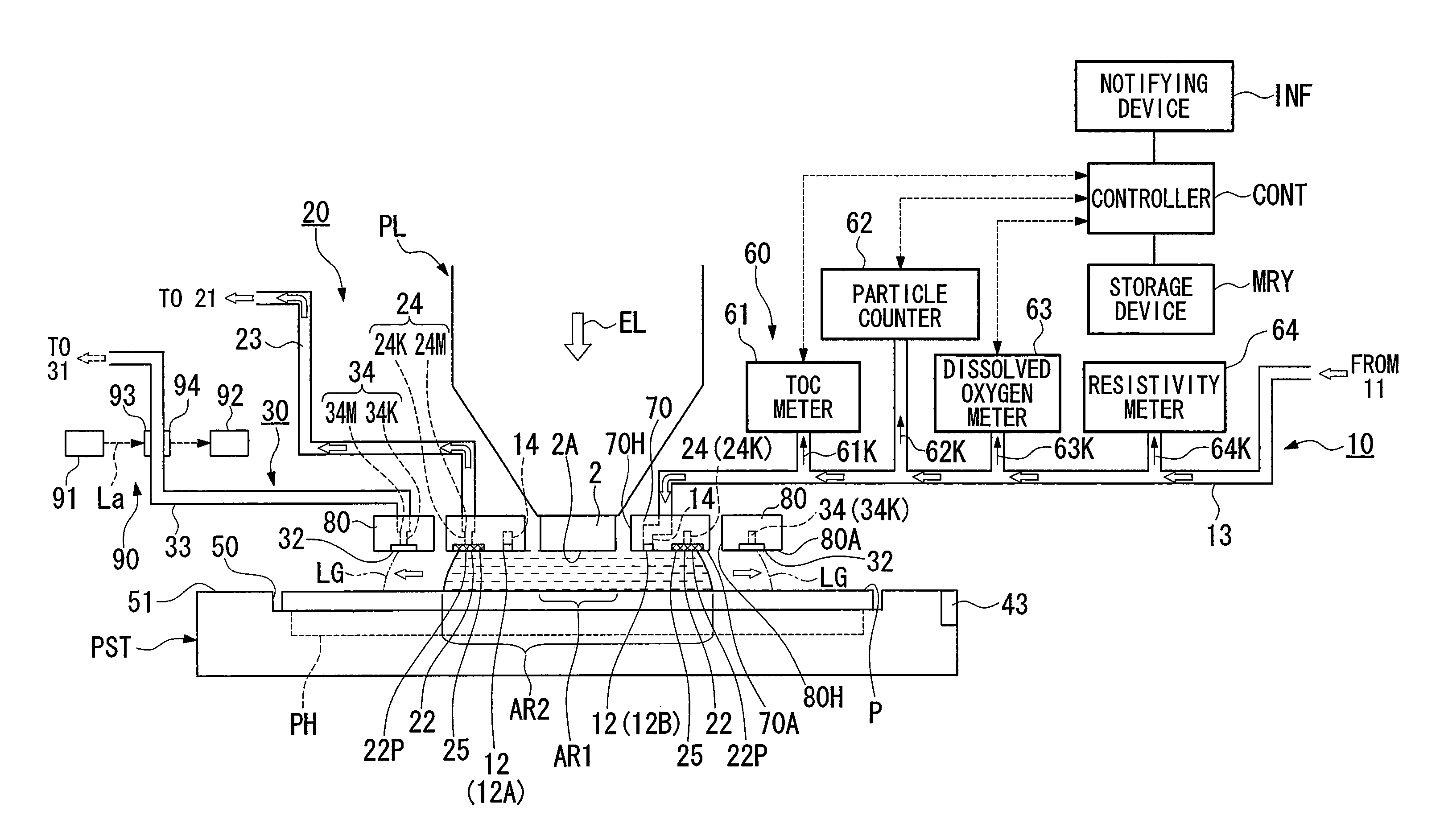
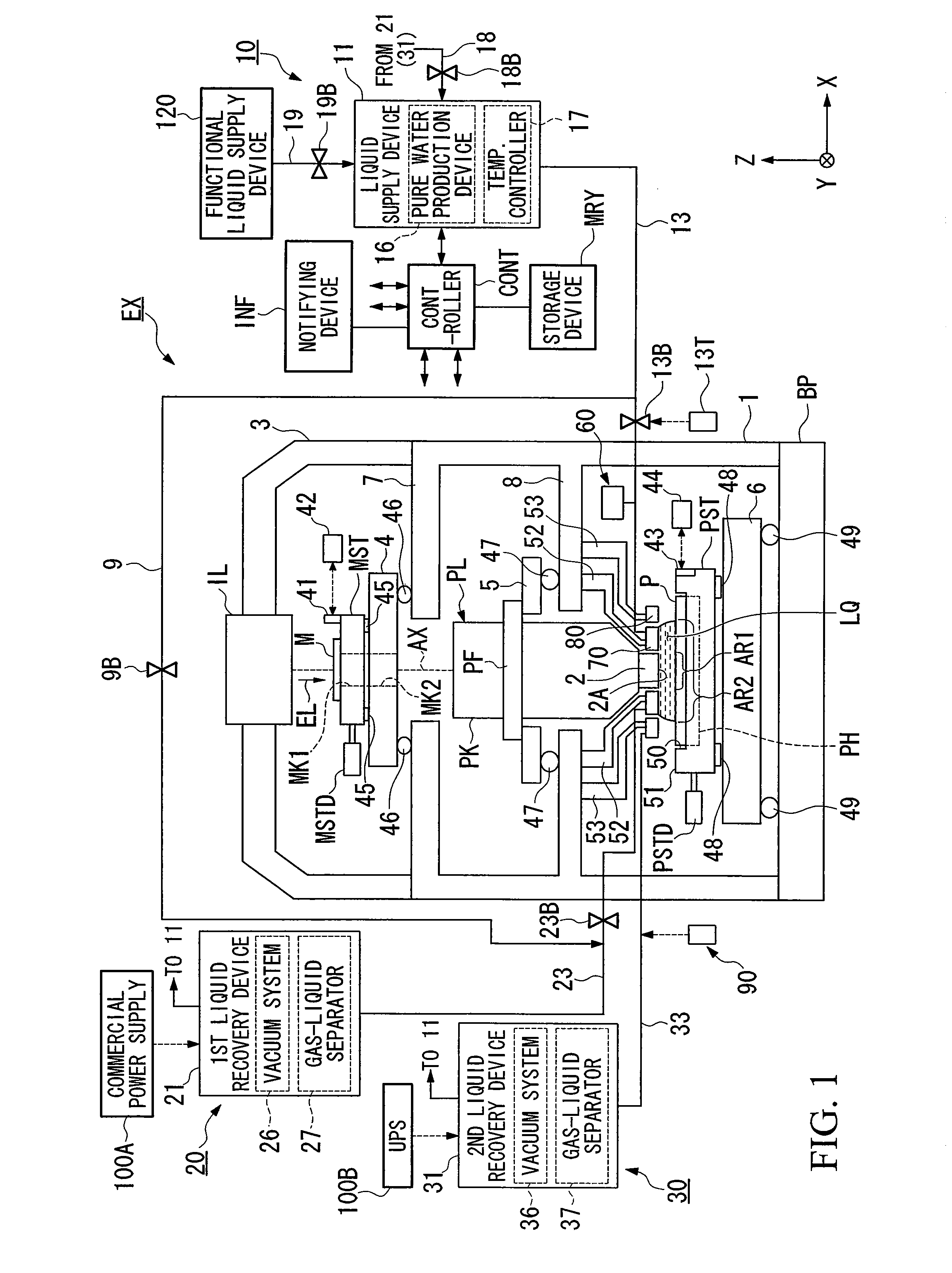
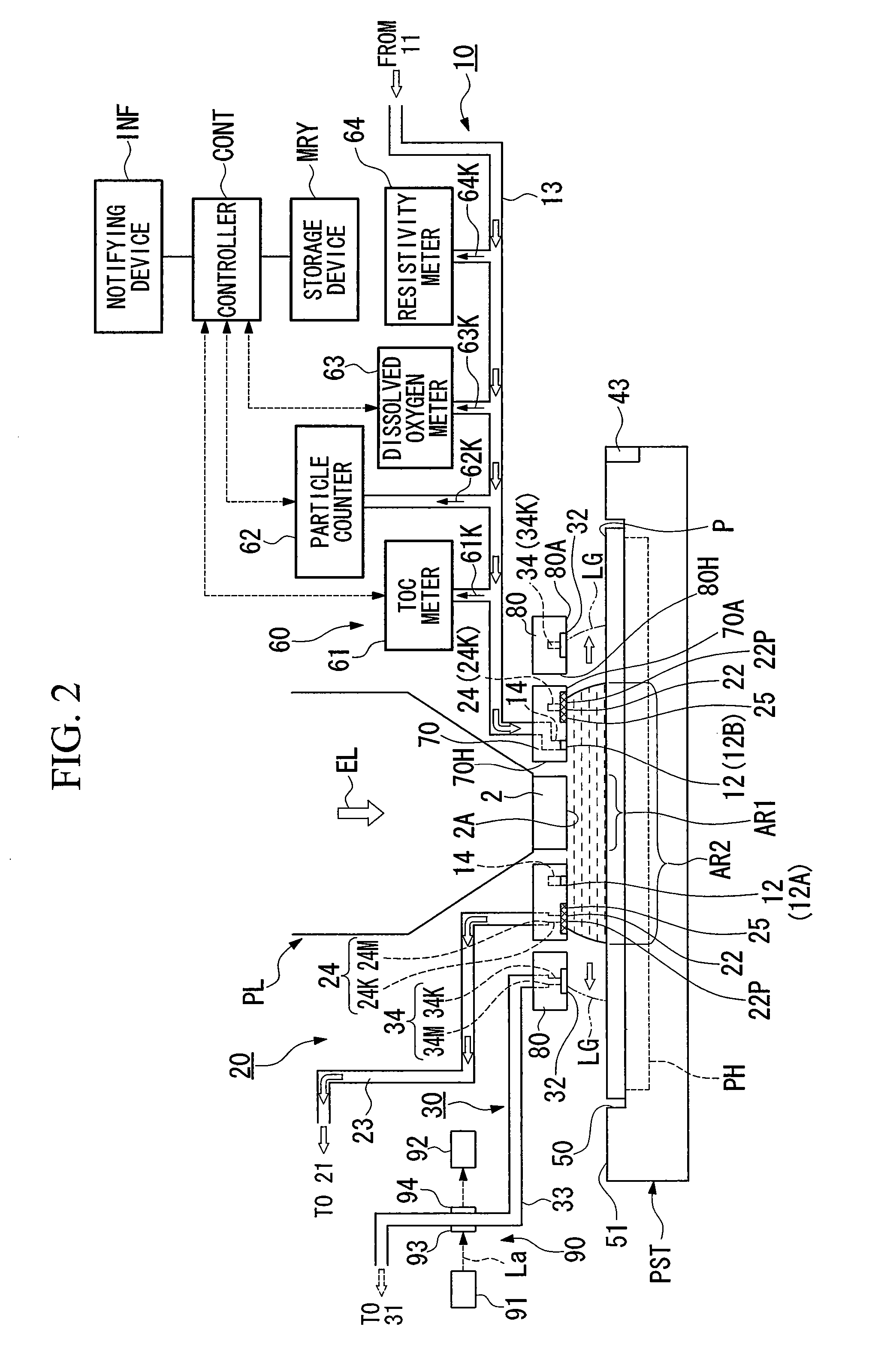
[0075] The exposure apparatus of the present invention will be described with reference to the drawings. FIG. 1 is a schematic block diagram showing one embodiment of the exposure apparatus of the present invention.
[0076] In FIG. 1, the exposure apparatus EX comprises a mask stage MST movable while holding a mask M, a substrate stage PST movable while holding a substrate P, an illumination optical system IL which illuminates the mask M held on the mask stage MST with exposure light EL, a projection optical system PL which projection-exposes a pattern image of the mask M illuminated with the exposure light EL onto the substrate P held on the substrate stage PST, and a controller CONT which centrally controls the whole operation of the exposure apparatus EX. A notifying device INF for reporting information relating to the exposure process is connected to the controller CONT. The notifying device INF includes an alarm device which issues a signal (warning) by using a display device, o...
PUM
| Property | Measurement | Unit |
|---|---|---|
| refractive index | aaaaa | aaaaa |
| wavelength | aaaaa | aaaaa |
| wavelength | aaaaa | aaaaa |
Abstract
Description
Claims
Application Information