X-Shaped Semiconductor Capacitor Structure

Active Publication Date: 2007-12-20
REALTEK SEMICON CORP
View PDF7 Cites 17 Cited by
  • Summary
  • Abstract
  • Description
  • Claims
  • Application Information

AI Technical Summary

Benefits of technology

[0012]It is therefore an object of the present invention to provide a semiconductor capacitor structure of be

Problems solved by technology

Although a multilevel interdigitated metal structure is already disclosed in U.S. Pat. No. 6,819,542, the electrical connection of the part of an electrode in the odd layer and the part of the same electrode in the eve

Method used


Image

  • X-Shaped Semiconductor Capacitor Structure
  • X-Shaped Semiconductor Capacitor Structure
  • X-Shaped Semiconductor Capacitor Structure

Examples


Embodiment Construction

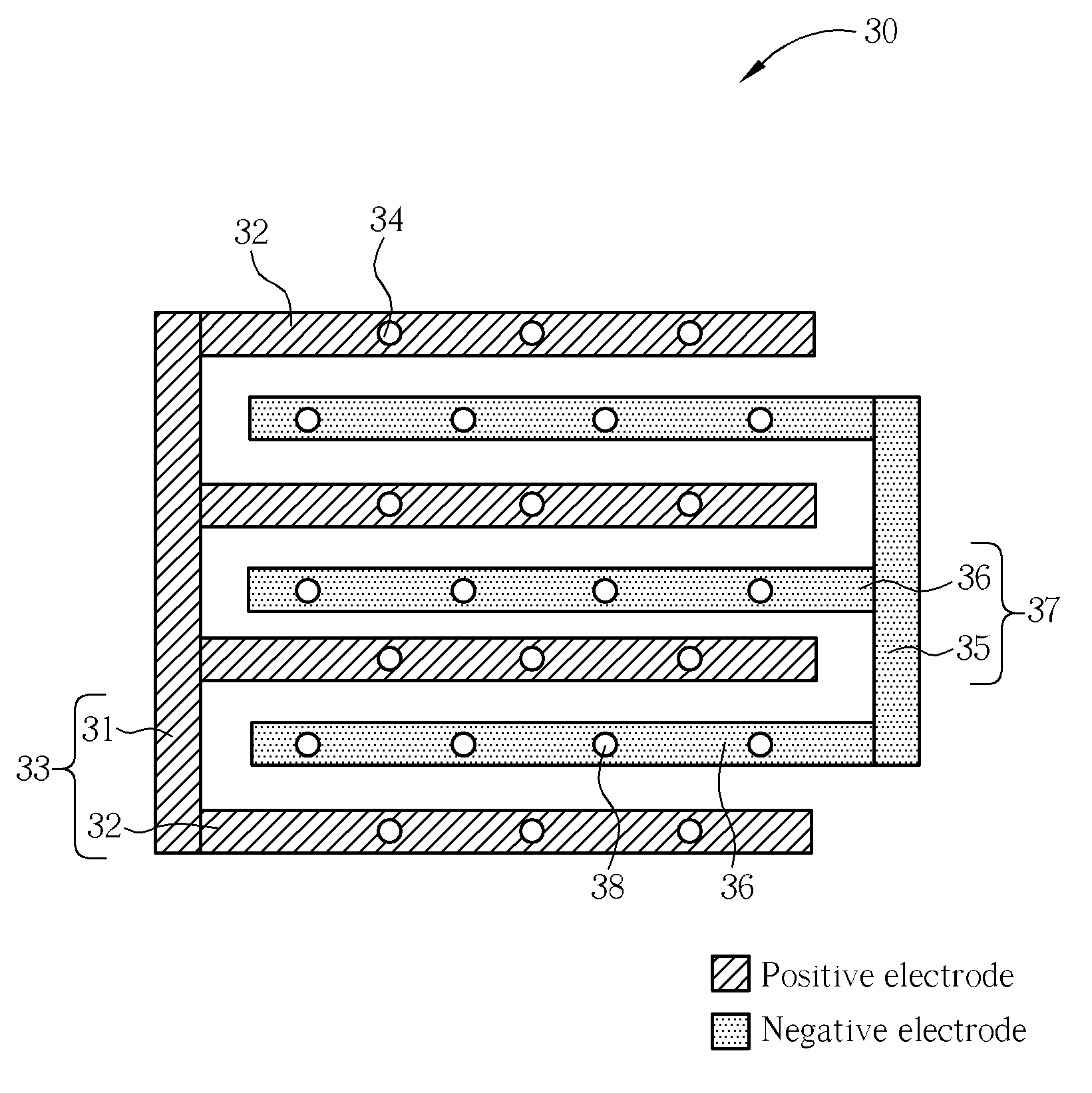
[0025]The semiconductor capacitor structures described in the embodiments of the invention adopt the capacitor manufacturing technologies embodying metal-insulator-metal (MIM) type structures, such as a metal-oxide-metal (MOM) structure. In other words, the capacitors in the embodiments of the present invention include metal layers as conductive material and insulator layers such as oxide layers as dielectric material. However, as would be appreciated by those of ordinary skill in the pertinent art, the realization of the core concept of the present invention is not necessarily limited to those disclosed in the embodiments as hereinafter described. Other known or novel conductive materials or dielectric materials can also be applied to implement the capacitor structure of the invention.

[0026]Please refer to FIG. 3. FIG. 3 is a diagram of a first metal layer 30 of an X-shaped semiconductor capacitor structure according to an embodiment of the present invention. The first metal layer ...


PUM


Abstract

A semiconductor capacitor structure includes a first metal layer, a second metal layer, a first set of via plugs, a second set of via plugs, and a dielectric layer. The first metal layer includes a first portion, a plurality of parallel-arranged second portions, a third portion, and a plurality of parallel-arranged fourth portions. The second metal layer includes a fifth section, a plurality of sixth sections, a seventh section, and a plurality of eighth sections. The first set of via plugs electrically connects the plurality of second sections to the plurality of sixth sections. The second set of via plugs electrically connects the plurality of fourth sections to the plurality of eighth sections.

Description

BACKGROUND OF THE INVENTION[0001]1. Field of the Invention[0002]The present invention relates to a semiconductor capacitor structure, and more particularly, to a metal-insulator-metal (MIM) type capacitor structure.[0003]2. Description of the Prior Art[0004]In semiconductor manufacturing processes, metal capacitors constituted by metal-insulator-metal (MIM) type capacitor structure are widely applied in Ultra Large Scale Integration (ULSI) designs. Due to its lower resistance, less significant parasitic effect, and absence of induced voltage shift in the depletion region, metal capacitors with MIM type structure are usually adopted as the main choice of semiconductor capacitor designs.[0005]Applications of interdigitated metal capacitors have already been disclosed and discussed in various literatures, such as U.S. Pat. No. 6,784,050, U.S. Pat. No. 6,885,543, U.S. Pat. No. 6,974,744, U.S. Pat. No. 6,819,542, and Taiwan Patent No. 222,089 (the Taiwan patent of U.S. Pat. No. 6,819,542...

Claims


Application Information

Patent Timeline
IPC IPC(8): H01G4/00
CPCH01L23/5223H01L27/0805H01L28/60H01L2924/0002H01L2924/00
Inventor YEH, TA-HSUN
Owner REALTEK SEMICON CORP
Why Eureka
Try Eureka