FFS mode liquid crystal display

a liquid crystal display and mode technology, applied in non-linear optics, instruments, optics, etc., can solve the problems of deterioration of the characteristics of manufactured goods, distortion of the operation of liquid crystal, and inferior afterimages, so as to improve the mura operation and improve the luminance. uniformity

Active Publication Date: 2007-12-27
HYDIS TECH CO LTD
View PDF3 Cites 3 Cited by
  • Summary
  • Abstract
  • Description
  • Claims
  • Application Information

AI Technical Summary

Benefits of technology

[0013] Accordingly, the present invention has been made to solve the above-mentioned problems occurring in the prior art, and an object of the present invention is to provide an FFS (Fringe Field Switching) mode liquid crystal display which can improve operating mura, luminance non-uniformity, etc., which have been problematic in the conventional FFS mode liquid crystal display, by establishing a new conception of mutual factors between a black matrix and a pixel electrode provided in an FFS design structure.

Problems solved by technology

According to the conventional FFS mode liquid crystal display fabricated the above-mentioned method, since an overlapped region between electrodes is very wide, layers such as an insulation layer may be deteriorated due to long-period electrical operations, which results in inferior afterimages.
However, according to conventional FFS pixels, the edge sections of the slit patterns having the wedge shape, which forms a non-uniform electric field (i.e. which causes distortion in the operation of liquid crystal) are not disposed in the black matrix but located in the actual transmission region.
As a result, such a relationship between the pixel wedge and the black matrix causes transmittance reduction and luminance non-uniformity due to an alternation operation between them, so that the characteristics of manufactured goods are deteriorated.

Method used


Image

  • FFS mode liquid crystal display
  • FFS mode liquid crystal display
  • FFS mode liquid crystal display

Examples


Embodiment Construction

[0019] Hereinafter, a preferred embodiment of the present invention will be described with reference to the accompanying drawings. In the following description and drawings, the same reference numerals are used to designate the same or similar components, and so repetition of the description on the same or similar components will be omitted.

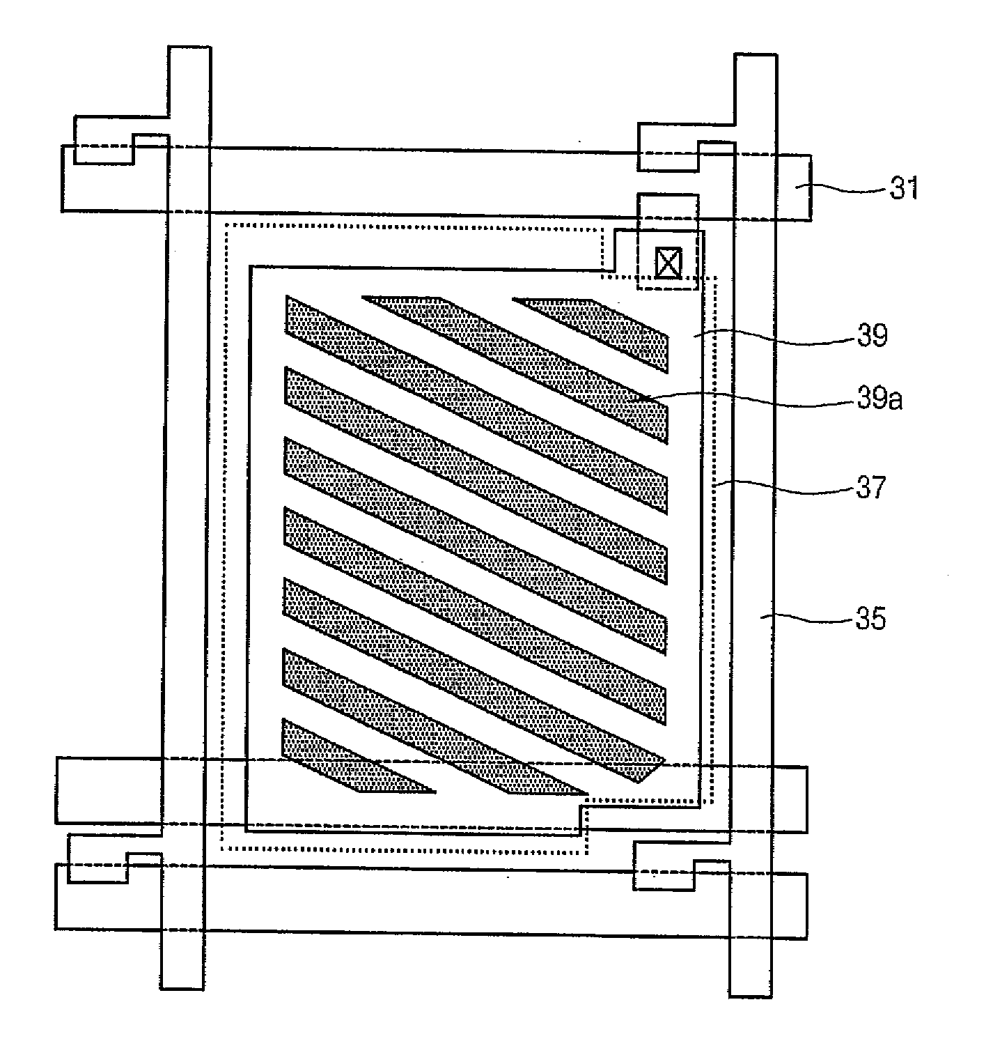
[0020]FIG. 2A is a layout view of an FFS (Fringe Field Switching) mode liquid crystal display according to one embodiment of the present invention, and FIG. 2B is a sectional view of the FFS mode liquid crystal display according to this embodiment of the present invention.

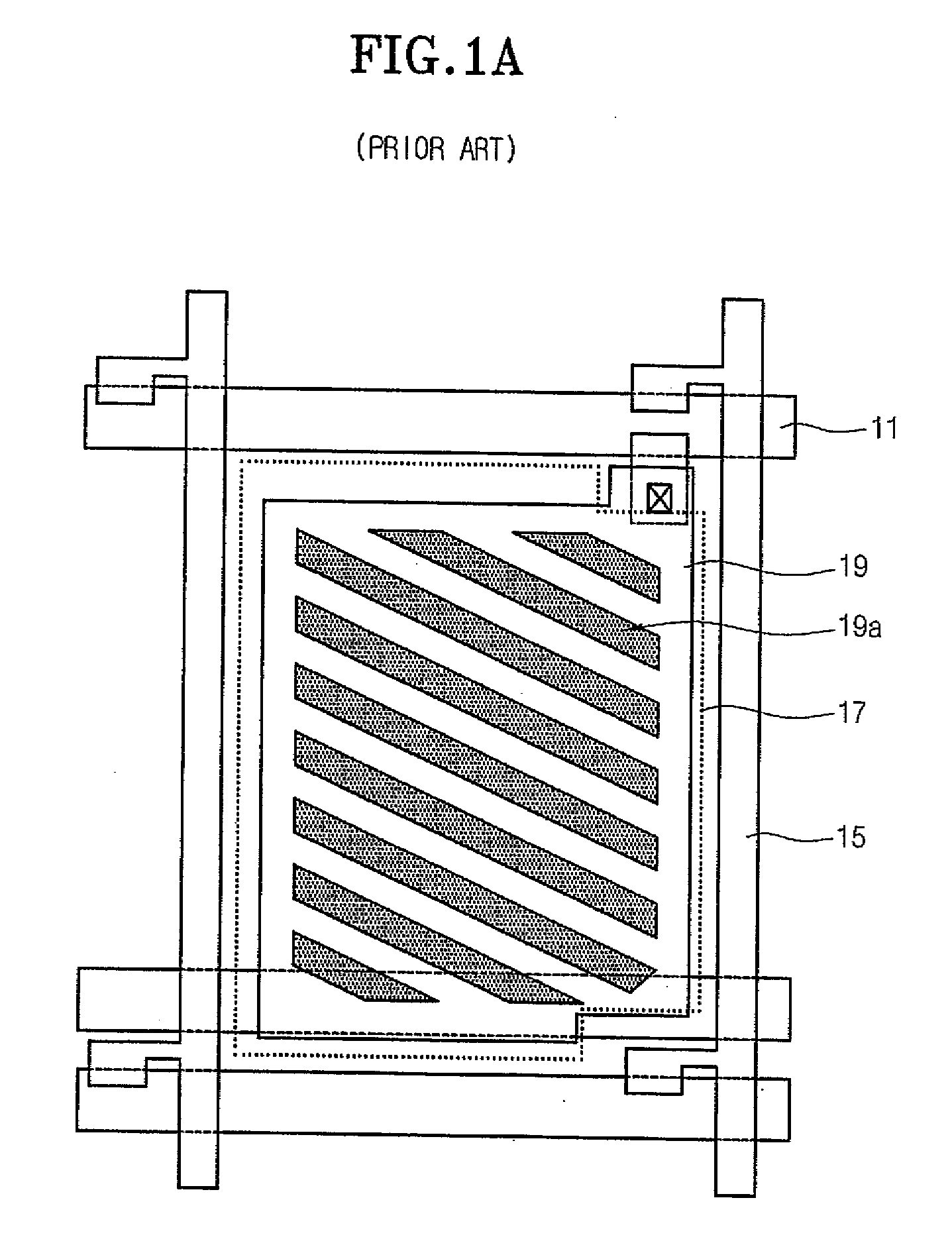
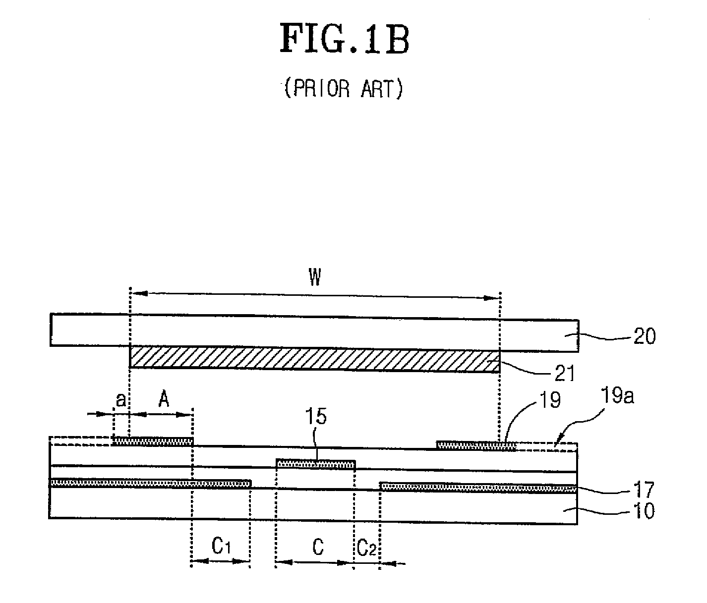
[0021]FIGS. 3 and 4 are schematic views for explaining FFS mode liquid crystal displays according to other embodiments of the present invention, in which a wedge portion of a second ITO electrode is formed with removed parts spaced from each other, so as to improve distortion of liquid crystal.

[0022] As shown in FIG. 2A according to an FFS mode liquid crystal display of one e...


PUM

PropertyMeasurementUnit
widthaaaaaaaaaa
lengthaaaaaaaaaa
widthaaaaaaaaaa

Abstract

An FFS (Fringe Field Switching) mode liquid crystal display comprises a lower substrate and an upper substrate and a gate line formed on the lower substrate. A data line crosses perpendicular to the gate line. A first ITO electrode is formed in a region defined by the gate line and the data line. A second ITO electrode of a comb-teeth pattern is formed on the lower substrate while being overlapped on the first ITO electrode. A black matrix formed on the upper substrate, wherein, a wedge portion of the second ITO electrode is formed at a position spaced by a predetermined interval to the inside from an edge section of the black matrix.

Description

RELATED APPLICATIONS [0001] This application is a continuation of U.S. patent application Ser. No. 10 / 883,422, which was filed on Jun. 30, 2004, and which is now abandoned.BACKGROUND OF THE INVENTION [0002] 1. Field of the invention [0003] The present invention relates to a fringe field switching (hereinafter, simply referred to as “FFS”) mode liquid crystal display, and more particularly to an FFS mode liquid crystal display capable of improving driving mura and luminance non-uniformity. [0004] 2. Description of the Prior Art [0005] A method for fabricating an ultra-FFS mode liquid crystal display may be described as follows, with reference to FIGS. 1A and 1B. Herein, FIG. 1A is a plan view of a conventional ultra-FFS mode liquid crystal display, and FIG. 1B is a sectional view thereof. [0006] As shown in FIG. 1A, according to the conventional ultra-FFS mode liquid crystal display, a gate line 11 and a data line 15 are aligned to cross perpendicular to each other on a lower substra...

Claims


Application Information

Patent Timeline
Patent Type & Authority Applications(United States)
IPC IPC(8): G02F1/1343G02F1/13357G02F1/1335G02F1/1368
CPCG02F1/134363G02F1/133512G02F1/1343
Inventor LEE, KYUNG HAKIM, HYANG YULJEON, JONG YOBAN, CHI WOOK
Owner HYDIS TECH CO LTD
Why Eureka
Try Eureka