

Shift register
a technology of shift register and shift register, which is applied in the direction of logic circuit, digital storage, instruments, etc., can solve the problems of deteriorating image quality of images displayed on the lcd panel
- Summary
- Abstract
- Description
- Claims
- Application Information
AI Technical Summary
Benefits of technology
Problems solved by technology
Method used
Image

Examples
first embodiment
[0042]FIG. 2 illustrates a shift register according to the present invention. FIG. 3 illustrates a timing view of signals supplied to and outputted from the shift register of FIG. 2.
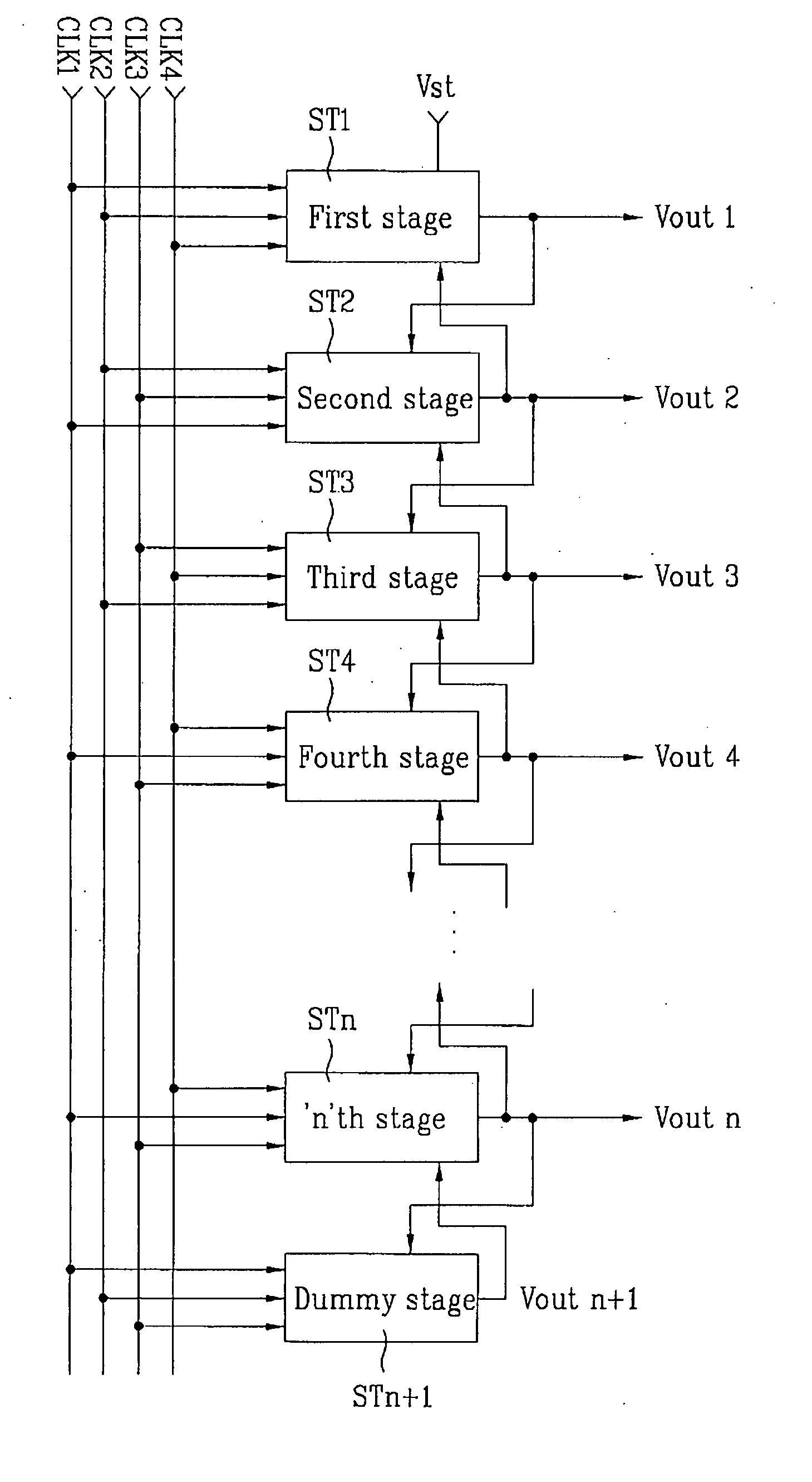
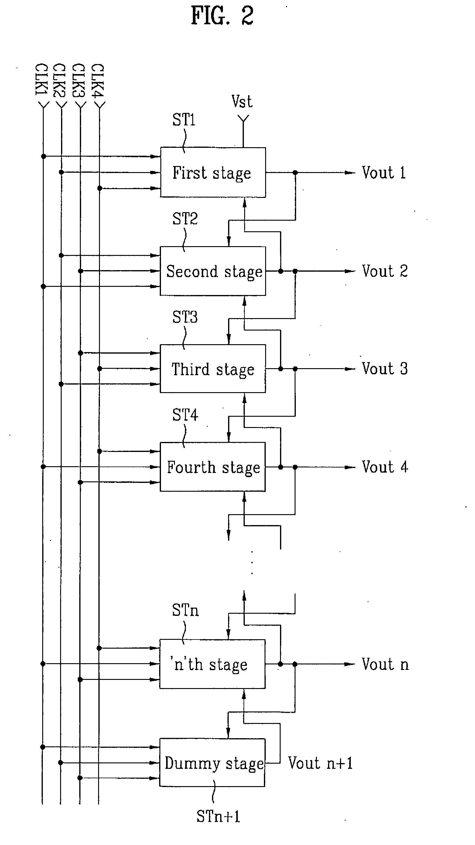
[0043] As shown in FIG. 2, the shift register according to the first embodiment of the present invention is comprised of ‘n’ stages (ST1 to STn) subordinately connected with one another, and one dummy stage (STn+1). At this time, each of the stages (ST1 to STn+1) outputs one output pulse (Vout1 to Voutn+1) during one frame. For example, the first to dummy stages (ST1 to STn+1) respectively output the output pulses in sequence. The output pulses (Vout1 to Voutn) outputted from the stages (ST1 to STn) except the dummy stage (STn+1) are sequentially supplied to the gate lines, to thereby scan the gate lines in sequence. That is, the first stage (ST1) outputs the first output pulse (Vout1) firstly; the second stage (ST2) outputs the second output pulse (Vout2) secondly; the third stage (ST3) outputs the thir...
second embodiment
[0111] Each of the stages (ST1 to STn+2) included in the shift register according to the present invention is supplied with the two clock pulses, wherein one is required to output the output pulse from each of the stages (ST1 to STn+2), and the other is required to control a noise eliminating unit 400 included in each of the stages (ST1 to STn+2).
[0112] To make each of the stages (ST1 to STn+2) output the output pulse, an enable node (Q) of each of the stages (ST1 to STn+2) is charged previously (that is, enable operation). For this, each of the stages (ST1 to STn+2) is supplied with the output pulse from the corresponding one positioned two stages ahead thereof, whereby each of the stages (ST1 to STn+2) charges its own enable node (Q). That is, in response to the output pulse from the ‘k−2’th stage, the ‘k’th stage charges the enable node (Q) of the ‘k’th stage with the charging voltage source (VDD). At this time, since there is no stage prior to the first stage (ST1) which is the ...
third embodiment
[0125]FIG. 18 illustrates a shift register according to the present invention.
[0126] The shift register according to the third embodiment of the present invention shown in FIG. 18 is identical in structure to the shift register shown in FIG. 15.
[0127] However, odd-numbered stages (ST1, ST3, . . . , STn+1) are positioned in the left side of the shift register, and even-numbered stages (ST2, ST4, . . . , STn+2) are positioned in the right side of the shift register. The odd-numbered stages (ST1, ST3, . . . , STn+1) drive odd-numbered gate lines, and the even-numbered stages (ST2, ST4, . . . , STn+2) drive even-numbered gate lines.
[0128] The odd-numbered stages (ST1, ST3, . . . , STn+1) are supplied with any two among first to fourth clock pulses, and the even-numbered stages (ST2, ST4, . . . , STn+2) are supplied with any two among the first to fourth clock pulses. The first to fourth clock pulses (CLK1 to CLK4) are outputted with the timing view of FIG. 6.
[0129] The noise eliminat...
PUM
 Abstract
Description
Claims
Application Information