Impedance control device and impedance control method

a technology of impedance control and impedance control, which is applied in the direction of amplifiers, semiconductor devices/discharge tubes, amplifiers, etc., can solve the problems of impedance mismatching with the transmission path, and achieve the effects of reducing manufacturing costs, short time period, and reducing circuit area

Inactive Publication Date: 2008-01-03
RENESAS ELECTRONICS CORP
View PDF11 Cites 7 Cited by
  • Summary
  • Abstract
  • Description
  • Claims
  • Application Information

AI Technical Summary

Benefits of technology

[0014]By including such configuration, the present invention can provide a semiconductor device and an impedance control method, which allow a reduction of a circuit area. From another viewpoint, a reduction of manufacturing costs can be realized. From further another viewpoint, it is possible to control input impedance and output impedance of the semiconductor device to a desired value in a short period of time.

Problems solved by technology

In an I / O interface connected to the transmission path, impedance mismatching with a transmission path is occurred due to impedance fluctuation caused by a manufacturing deviations or temperature dependency of elements such as a transistor and resistor disposed in a terminal of the interface and fluctuation of a power supply voltage or the like.

Method used


Image

  • Impedance control device and impedance control method
  • Impedance control device and impedance control method
  • Impedance control device and impedance control method

Examples


first embodiment

2. First Embodiment

(Configuration of the Substrate Bias Control Circuits 20 and 30)

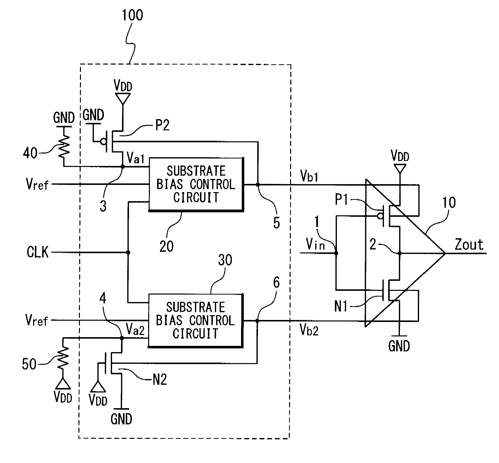
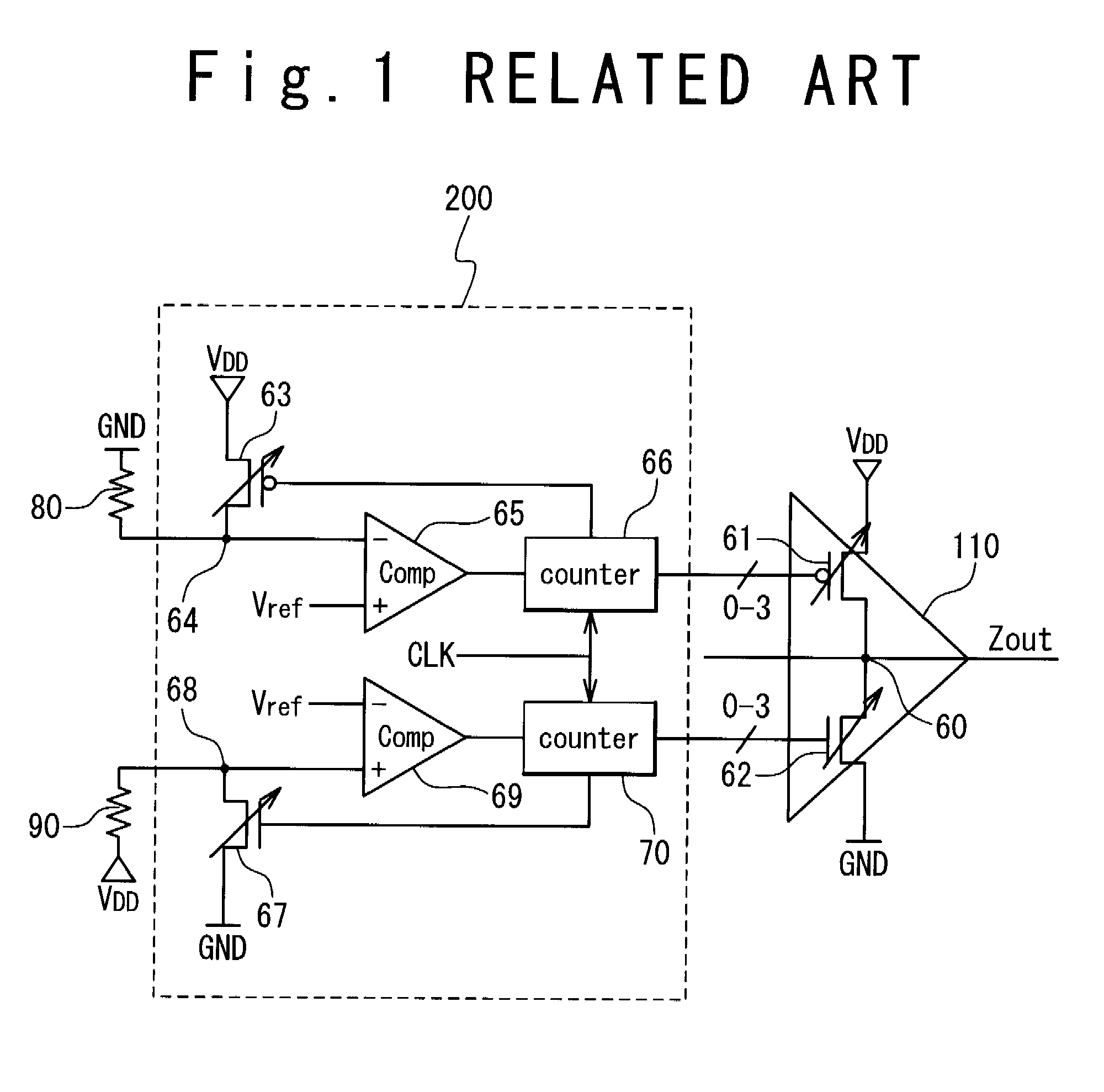
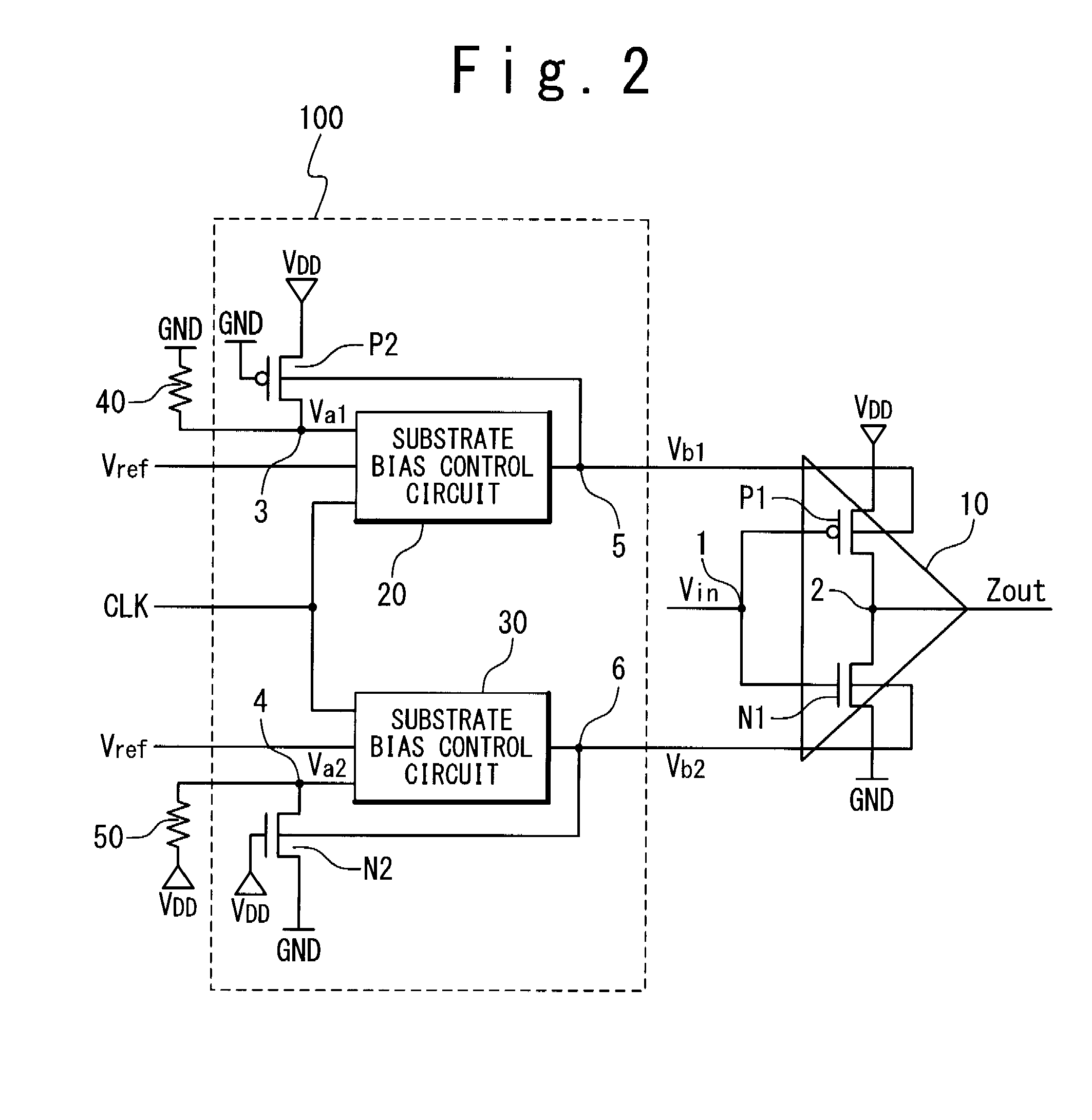
[0029]FIG. 3 is a block diagram showing the configuration in first embodiment of the substrate bias control circuits 20 and 30 according to the present invention. Referring to FIG. 3, the configuration in the first embodiment of the substrate bias control circuits 20 and 30 is explained. The substrate bias control circuit 20 in this embodiment is provided with a comparator 21, an up-down counter (referred to as a counter hereinafter) 22, and a D / A converter (referred to as a DAC hereinafter) 23. The divided voltage Va1 is supplied to the inverted input terminal of the comparator 21, and the reference voltage Vref is supplied to the non-inverted input terminal thereof. The comparator 21 outputs the result of comparison between the divided voltage Va1 and the reference voltage Vref to the counter 22. The counter 22 counts up or counts down a counter value (binary value) on the basis of the comparison re...

second embodiment

3. Second Embodiment

(Configuration of the Substrate Bias Control Circuits 20 and 30)

[0041]FIG. 5 is a block diagram showing the configuration in second embodiment of the substrate bias control circuits 20 and 30 according to the present invention. Referring to FIG. 5, the second embodiment of the substrate bias control circuits 20 and 30 is explained below. The substrate bias control circuit 20 in the present embodiment is configured to further include a filter 24 in addition to the substrate bias control circuit 20 in the first embodiment. The filter 24 is interposed between the comparator 21 and the counter 22, and extracts an appropriate value as a comparison result from the comparison result outputted from the comparator 21 in order to output to the counter 22. The counter 22 counts up or counts down the count value on the basis of a value (which is a filtered comparison result) inputted from the filter 24. The DAC 23 applies D / A conversion to the count value obtained from the c...


PUM


Abstract

A compact semiconductor device for controlling impedance is provided. The semiconductor device has: a replica transistor of a transistor included in a control target circuit; and a substrate bias control circuit for controlling the impedance of the control target circuit by applying a substrate bias potential to the transistor in the control target circuit. The substrate bias potential is fed back to the substrate bias control circuit via the replica transistor.

Description

BACKGROUND OF THE INVENTION[0001]1. Field of the Invention[0002]The present invention relates to a semiconductor device, particularly an impedance control circuit and an impedance control method in which the input impedance or output impedance of a controlled object circuit is controlled to a desired value.[0003]2. Description of Related Art[0004]In recent years, impedance matching between a semiconductor device and a transmission path has become increasingly important in a field of a high-speed interface represented by the SerDes (Serializer / Deserializer) in accordance with implementation of high-speed operations of semiconductor devices. In an I / O interface connected to the transmission path, impedance mismatching with a transmission path is occurred due to impedance fluctuation caused by a manufacturing deviations or temperature dependency of elements such as a transistor and resistor disposed in a terminal of the interface and fluctuation of a power supply voltage or the like.[0...

Claims


Application Information

Patent Timeline
Patent Type & Authority Applications(United States)
IPC IPC(8): H03F3/26
CPCH03K19/0005
Inventor TSUJIGAWA, TAKURO
Owner RENESAS ELECTRONICS CORP
Why Eureka
Try Eureka