Check patentability & draft patents in minutes with Patsnap Eureka AI!

Semiconductor memory and address-decoding circuit and method for decoding address

a technology of address decoding and memory, applied in the direction of static storage, digital storage, instruments, etc., can solve the problems of increasing the fabrication cost, defective memory cells of the above-mentioned fabrication process, etc., and achieve the effect of reducing memory capacity and reducing capacity

Active Publication Date: 2008-01-03
WINBOND ELECTRONICS CORP
View PDF15 Cites 2 Cited by
  • Summary
  • Abstract
  • Description
  • Claims
  • Application Information

AI Technical Summary

Benefits of technology

[0006]One aspect of the present invention provides a semiconductor memory and address-decoding circuit and method for decoding address, which allows the semiconductor memory to operate under a decreased capacity by disabling or hiding a predetermined portion of the semiconductor memory.
[0010]The semiconductor memory of the present invention can use the address-setting bit to set a sector-selecting bit of the internal address such that a portion of the semiconductor memory can be hidden to decrease the memory capacity or disable memory units with defects, and the semiconductor memory is allowed to operate under a decreased capacity. In particular, the present invention can disable a predetermined memory sector under the same memory hierarchy without affecting the original accessing function of the semiconductor memory.

Problems solved by technology

However, it is unavoidable that some of the semiconductor memories prepared by the above fabrication process have defective memory cells without normal access function due to process variation.
The manufacture of semiconductor memory requires different fabrication processes to manufacture different semiconductor memories of different capacities, which increases the fabrication cost.

Method used


Image

  • Semiconductor memory and address-decoding circuit and method for decoding address
  • Semiconductor memory and address-decoding circuit and method for decoding address
  • Semiconductor memory and address-decoding circuit and method for decoding address

Examples


Embodiment Construction

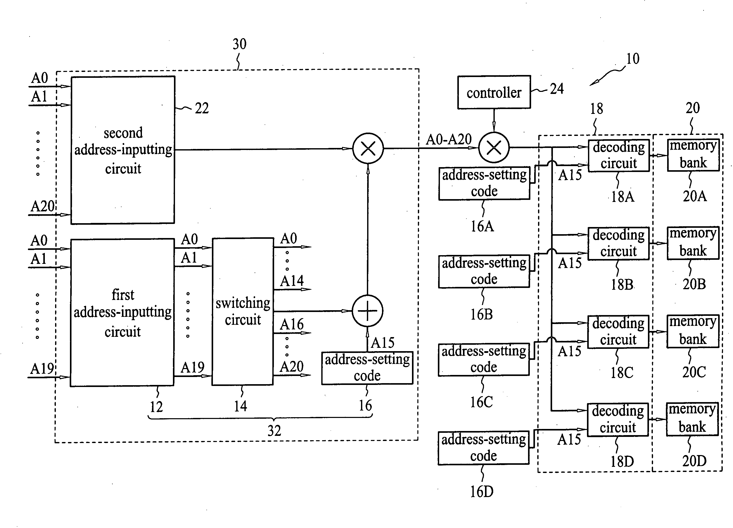
[0016]FIG. 1 and FIG. 2 illustrate a semiconductor memory 10 according to one embodiment of the present invention. The semiconductor memory 10 comprises a first address-inputting circuit 12 configured to receive a first external address (20 bits, A0-A19), a second address-inputting circuit 22 configured to receive a second external address (21 bits, A0-A20), a switching circuit 14 configured to switch a predetermined portion of the first external address to form an internal address (21 bits, A0-A20), at least one address-setting code 16 configured to set at least one predetermined bit of the internal address, a decoder 18 coupling to the switching circuit 14 and the address-setting code 16, a memory array 20 coupling to the decoder 18 and a controller 24 configured to control the access of the semiconductor memory 10. In particular, the first address-inputting circuit 12, the switching circuit 14 and the address-setting code 16 can be considered as a address-decoding circuit 32, and...


PUM


Abstract

A semiconductor memory and address-decoding circuit and method for decoding address allow the semiconductor memory to operate under a decreased capacity by disabling or hiding a predetermined portion of the semiconductor memory. The semiconductor memory comprises a first address-inputting circuit configured to receive a first external address, a switching circuit configured to switch a predetermined portion of the first external address to form an internal address, at least one address-setting code configured to set at least one predetermined bit of the internal address, a decoder coupling to the switching circuit and the address-setting code, and a memory array coupling to the decoder, wherein the decoder is configured to select at least one memory unit of the memory array based on the internal address. The first address-inputting circuit, the switching circuit and the address-setting code can be considered as an address-decoding circuit.

Description

BACKGROUND OF THE INVENTION[0001](A) Field of the Invention[0002]The present invention relates to a semiconductor memory and address-decoding circuit and method for decoding address, and more particularly, to a semiconductor memory and address-decoding circuit and method for decoding address by setting at least one bit of the address to disable a predetermined portion of the semiconductor memory.[0003](B) Description of the Related Art[0004]The semiconductor memory is prepared by a series of fabrication processes such as lithographic process, etching process, and deposition process to form memory units and accessing circuits on the wafer, which is then sliced into several die and encapsulated after testing. However, it is unavoidable that some of the semiconductor memories prepared by the above fabrication process have defective memory cells without normal access function due to process variation.[0005]Generally, semiconductor memory units with defective memory cells are pulled out ...

Claims


Application Information

Patent Timeline
Patent Type & Authority Applications(United States)
IPC IPC(8): G11C8/00
CPCG11C8/10
Inventor MOU, CHI YUANLU, CHIEN HAOHSIEH, WEN PINCHANG, YA CHUN
Owner WINBOND ELECTRONICS CORP
Features
  • R&D
  • Intellectual Property
  • Life Sciences
  • Materials
  • Tech Scout
  • Unparalleled Data Quality
  • Higher Quality Content
  • 60% Fewer Hallucinations
Learn More