

Programmable metallization cell structures including an oxide electrolyte, devices including the structure and method of forming same
a metallization cell and oxide electrolyte technology, applied in semiconductor devices, digital storage, instruments, etc., can solve the problems of high cost of manufacture, large energy consumption for data storage, and particularly volatile dynamic ram (“dram”), so as to improve the speed of the read/write process
- Summary
- Abstract
- Description
- Claims
- Application Information
AI Technical Summary
Benefits of technology
Problems solved by technology
Method used
Image

Examples
Embodiment Construction
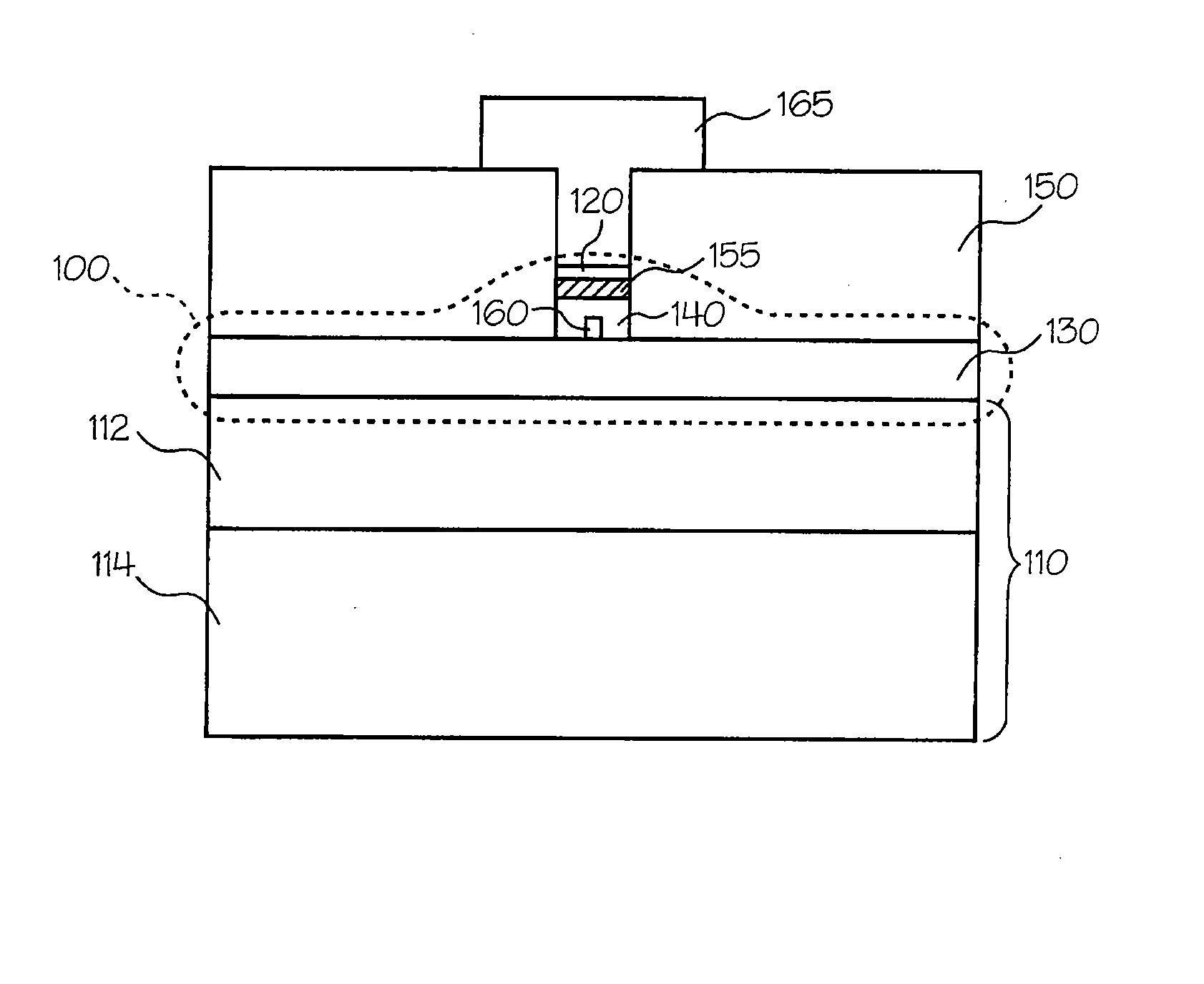
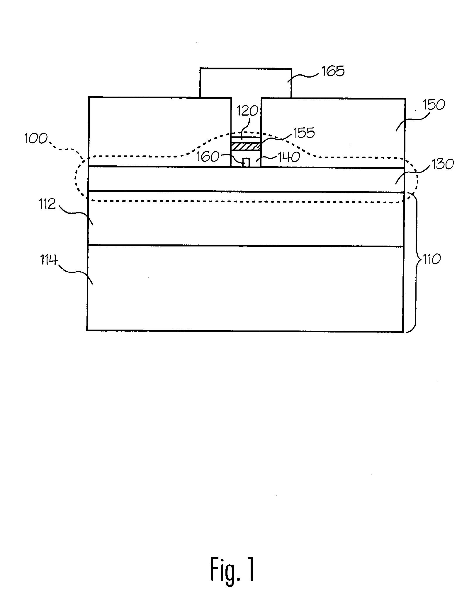
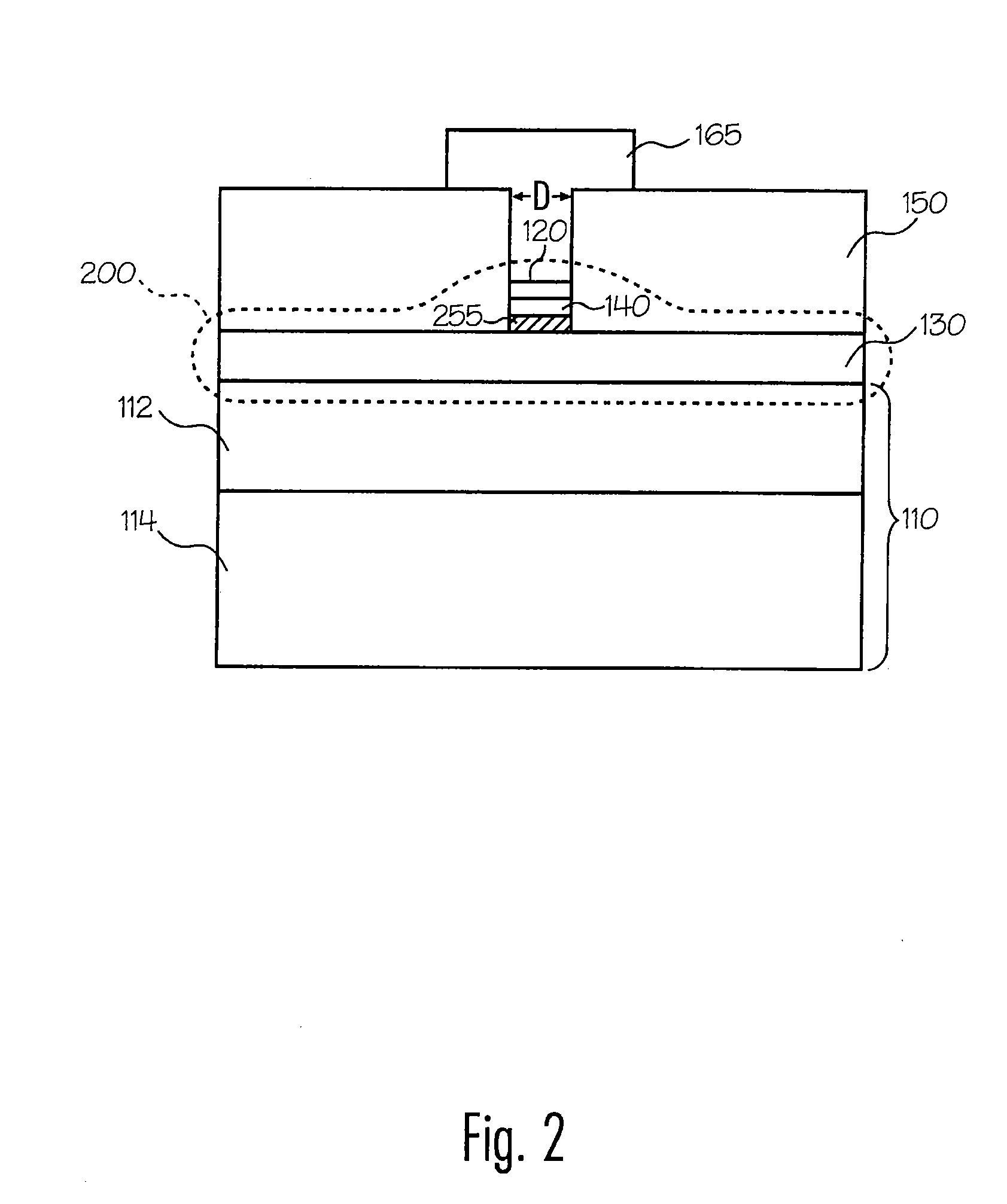
[0037] The present invention generally relates to programmable microelectronic structures and devices, to arrays including the structures and devices, and to methods of forming and using the devices and arrays.
[0038]FIGS. 1 and 2 illustrate programmable microelectronic structures 100 and 200 formed on a surface of a substrate 110 in accordance with an exemplary embodiment of the present invention. Structures 100 and 200 include electrodes 120 and 130, an ion conductor 140, and optionally include buffer or barrier layers or regions 155 and / or 255.
[0039] Generally, structures 100 and 200 are configured such that when a bias greater than a threshold voltage (VT), discussed in more detail below, is applied across electrodes 120 and 130, the electrical properties of structure 100 change. For example, in accordance with one embodiment of the invention, as a voltage V≧VT is applied across electrodes 120 and 130, conductive ions within ion conductor 140 begin to migrate and form a region ...
PUM
 Abstract
Description
Claims
Application Information