

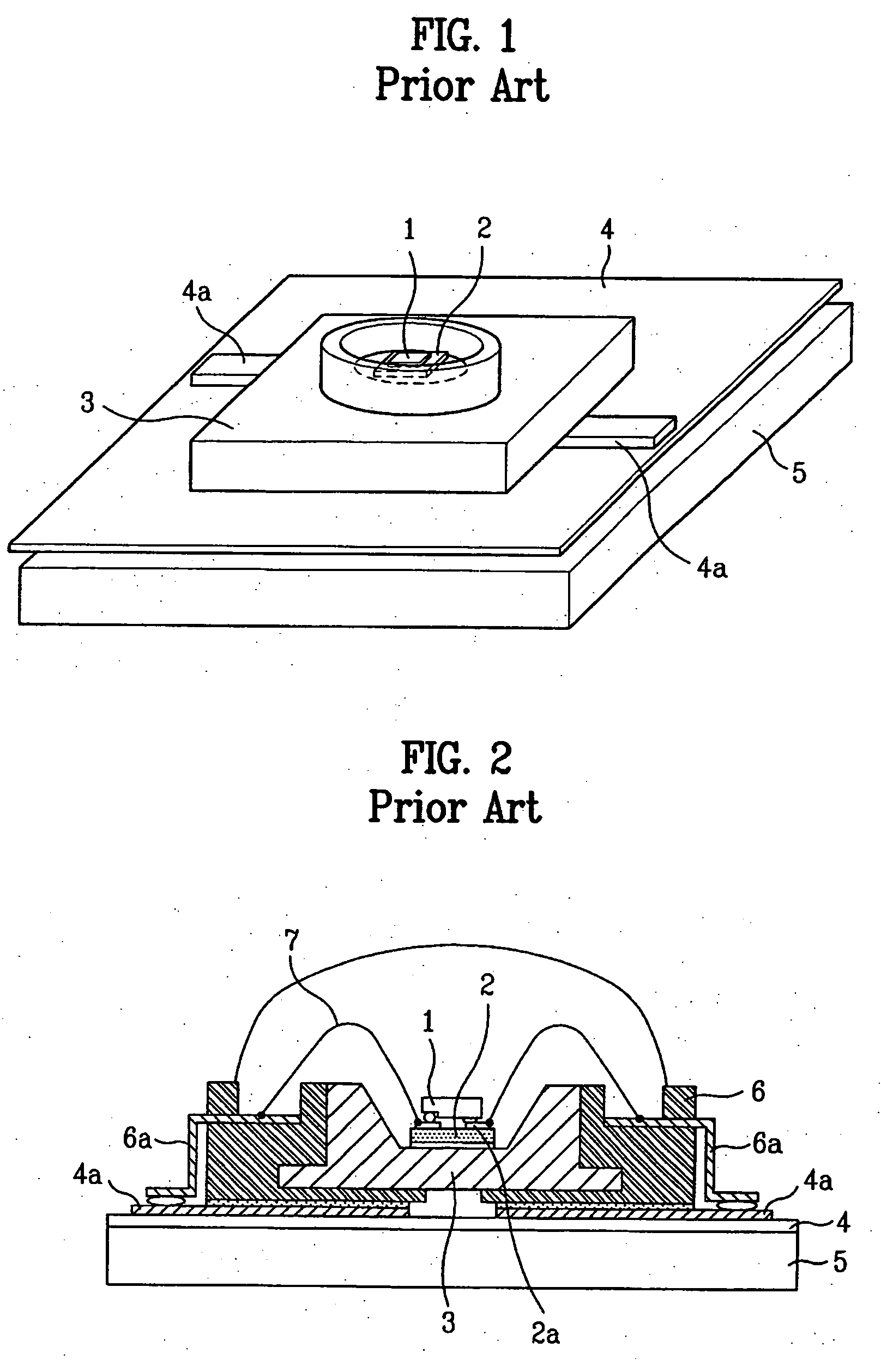
Sub-mount for mounting light emitting device and light emitting device package
a technology of light emitting devices and sub-mounts, which is applied in the direction of semiconductor devices, basic electric elements, electrical appliances, etc., can solve the problems of difficult implementation of illumination apparatus such as backlights, degraded and reduced heat discharge, so as to achieve low heat transfer rate and reduce the effect of optical characteristics of leds
- Summary
- Abstract
- Description
- Claims
- Application Information
AI Technical Summary
Benefits of technology
Problems solved by technology
Method used
Image

Examples
first embodiment
[0080]
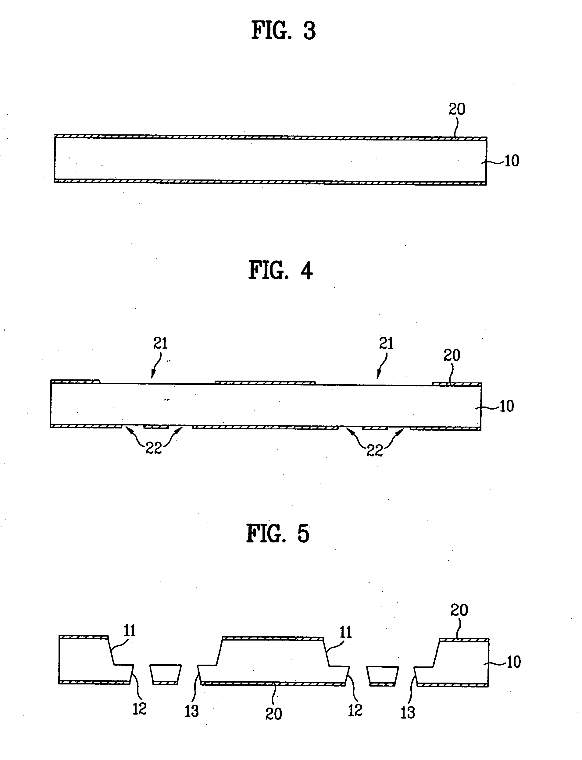
[0081]First, a procedure for forming a mount 11, for example, a recess-shaped or groove shaped mount, on which a light emitting device will be mounted, and through holes 12 and 13 will be described with reference to FIGS. 3 to 6.
[0082]In this procedure, a substrate is first prepared, as shown in FIG. 3. The substrate 10 may include a silicon substrate, or substrates made of other materials, namely, aluminum, aluminum nitride (AlN), aluminum oxide (AlOx), photo sensitive glass (PSG), Al2O3, and BeO. The substrate 10 may be a PCB substrate.
[0083]Mask layers 20 made of, for example, a photoresist material, are then formed over opposite major surfaces of the prepared substrate 10. Alternatively, a substrate, on which the mask layers 20 have previously been formed, may be prepared as the substrate 10. As shown in FIG. 4, the mask layers 20 are then patterned to form mask patterns required for bulk-etching of a region where a light emitting device will be mounted, namely, a region w...
second embodiment
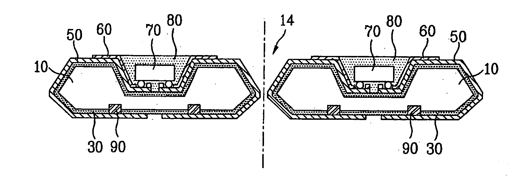
[0143]FIG. 15 illustrates an embodiment in which a light emitting device 72 is bonded to the substrate 10 in accordance with a wire bonding process using wires 73, differently from the case of FIG. 14.
[0144]In particular, where a vertical light emitting device 72 having electrodes at the top and bottom thereof is used, the lower electrode of the light emitting device 72 is bonded to one of the front electrodes 50a via a wire 73, whereas the upper electrode of the light emitting device 72 is bonded to the other front electrode 50a having a polarity opposite to that of the one-side front electrode 50a via a wire 73.
[0145]The remaining fabrication processes and structures of this embodiment are similar to those of the first embodiment.
third embodiment
[0146]FIG. 16 illustrates a structure in which the mount 11 or each through hole 12 or 13 of the light emitting device 70 has a vertical surface in accordance with a third embodiment of the present invention.
[0147]In accordance with this embodiment, the mount 11 or each through hole 12 or 13 may be formed to have a vertical surface other than an inclined surface, in accordance with a laser drilling method or a deep-RIE method.
[0148]The mount 11 or each through hole 12 or 13 having a vertical surface can be formed in accordance with a wet etching method under the condition in which a silicon substrate having a [110] orientation is used for the substrate 10.
[0149]When the through holes 12 and 13 have vertical surfaces, respectively, it is possible to more easily enable the front electrode 50a and rear electrode 50b to come into contact with each other via the through holes 12 and 13.
PUM
 Abstract
Description
Claims
Application Information