Nonvolatile memory device and methods of operating and fabricating the same

a nonvolatile memory and memory device technology, applied in semiconductor devices, digital storage, instruments, etc., can solve the problems of short channel effect, limited operation current reduction of conventional nonvolatile memory devices, and high operating current requirements of nonvolatile memory devices using resistive nodes, etc., to achieve lower operating current, higher integration, and higher speed

Active Publication Date: 2008-01-17
SAMSUNG ELECTRONICS CO LTD
View PDF3 Cites 63 Cited by
  • Summary
  • Abstract
  • Description
  • Claims
  • Application Information

AI Technical Summary

Benefits of technology

[0009]Example embodiments provide a nonvolatile memory device and having a lower operating current and/or enabling higher integration and higher sp...

Problems solved by technology

However, nonvolatile memory devices using resistive nodes require a higher operating current.
Accordingly, conventional nonvolatile memory devices may ha...

Method used


Image

  • Nonvolatile memory device and methods of operating and fabricating the same
  • Nonvolatile memory device and methods of operating and fabricating the same
  • Nonvolatile memory device and methods of operating and fabricating the same

Examples


Embodiment Construction

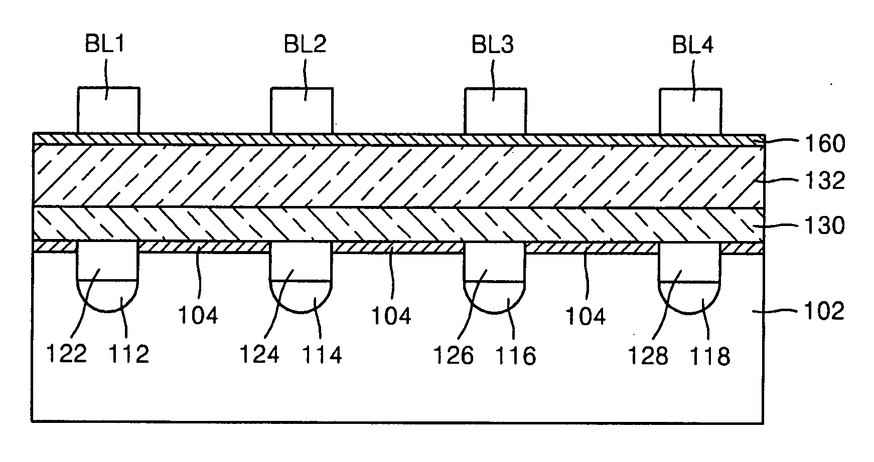
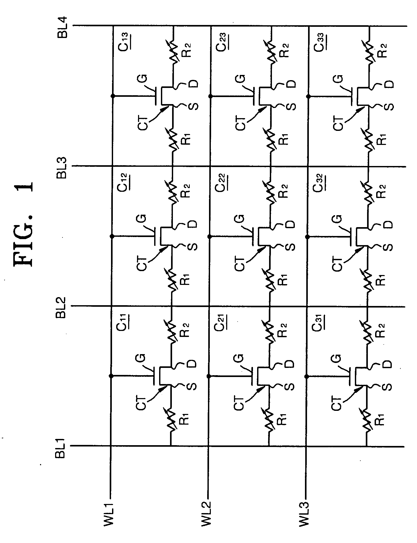
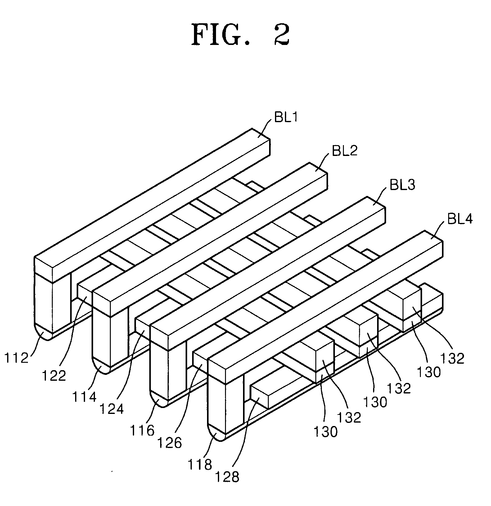
[0027]Reference will now be made in detail to example embodiments, examples of which are illustrated in the accompanying drawings. However, example embodiments are not limited to the embodiments illustrated hereinafter, and the embodiments herein are rather introduced to provide easy and complete understanding of the scope and spirit of example embodiments. In the drawings, the thicknesses of layers and regions are exaggerated for clarity.

[0028]It will be understood that when an element or layer is referred to as being “on,”“connected to” or “coupled to” another element or layer, it may be directly on, connected or coupled to the other element or layer or intervening elements or layers may be present. In contrast, when an element is referred to as being “directly on,”“directly connected to” or “directly coupled to” another element or layer, there are no intervening elements or layers present. Like reference numerals refer to like elements throughout. As used herein, the term “and / or...


PUM


Abstract

Provided is a nonvolatile memory device and method of operating and fabricating the same for higher integration and higher speed, while allowing for a lower operating current. The nonvolatile memory device may include a semiconductor substrate. Resistive layers each storing a variable resistive state may be formed on the surface of the semiconductor substrate. Buried electrodes may be formed on the semiconductor substrate under the resistive layers and may connect to the resistive layers. Channel regions may be formed on the surface of the semiconductor substrate and connect adjacent resistive layers to each other, but not to the buried electrodes. Gate insulating layers may be formed on the channel regions of the semiconductor substrate. Gate electrodes may be formed on the gate insulating layers and extend over the resistive layers.

Description

PRIORITY STATEMENT[0001]This application claims priority under 35 USC § 119 to Korean Patent Application No. 2006-0036408, filed on Apr. 21, 2006, in the Korean Intellectual Property Office (KIPO), the entire contents of which are herein incorporated by reference.BACKGROUND[0002]1. Field[0003]Example embodiments relate to a nonvolatile memory device including resistive nodes and methods of operating and fabricating the same.[0004]2. Description of the Related Art[0005]Nonvolatile memory devices (e.g., phase-change RAM (PRAM) devices or resistance RAM (RRAM) devices) operate by varying the resistance of resistive nodes. As semiconductor products demand higher data capacity, higher integration and more operation bits of the nonvolatile memory device may be required. As such, multi-bit nonvolatile memory devices are increasingly required.[0006]Because faster data processing speed may be required to process extra data, it is necessary for nonvolatile memory devices to have higher operat...

Claims


Application Information

Patent Timeline
IPC IPC(8): H01L29/76
CPCG11C13/0004G11C13/0007G11C13/003G11C13/0069G11C16/0475H01L27/24G11C2213/31G11C2213/32G11C2213/71G11C2213/76G11C2013/0073H10B63/84H10B63/30H10B63/80H10N70/823H10N70/20H10N70/8836H10N70/231H10N70/066H10N70/8828H10N70/8833H10B63/00
Inventor PARK, YOON-DONGLEE, MYOUNG-JAEKIM, DONG-CHULAHN, SEUNG-EON
Owner SAMSUNG ELECTRONICS CO LTD
Why Eureka
Try Eureka