Single gate pole non-volatile internal storage and its operation method

A non-volatile, method-of-operation technology, applied in the field of non-volatile memory, which can solve the problem of reducing the current requirement of programming single gate

Active Publication Date: 2007-10-10
YIELD MICROELECTRONICS CORP
View PDF0 Cites 5 Cited by
  • Summary
  • Abstract
  • Description
  • Claims
  • Application Information

AI Technical Summary

Problems solved by technology

[0004] In view of the above problems, the main purpose of the present invention is to provide a single gate non-volatile memory and its operation method, which uses a single floating gate structure, and when programming, a real useful voltage is applied to the source Or apply a back bias to the transistor base to generate a wider depleted source-substrate junction, thereby improving the efficiency of current flow to the floating gate, so as to greatly reduce the non-volatile memory of the programmed single gate. current demand

Method used


Image

  • Single gate pole non-volatile internal storage and its operation method
  • Single gate pole non-volatile internal storage and its operation method
  • Single gate pole non-volatile internal storage and its operation method

Examples


no. 5 example

[0135] In addition, the present invention also provides a fifth embodiment, which uses a negative voltage applied to the P-type well, so that the absolute voltage of the drain or gate becomes smaller (less than 5V) during programming and erasing, so as to achieve low voltage and low consumption The operating effect of the current.

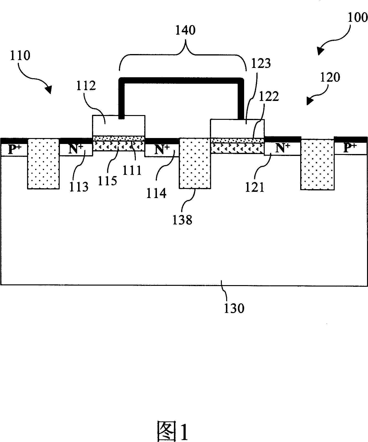
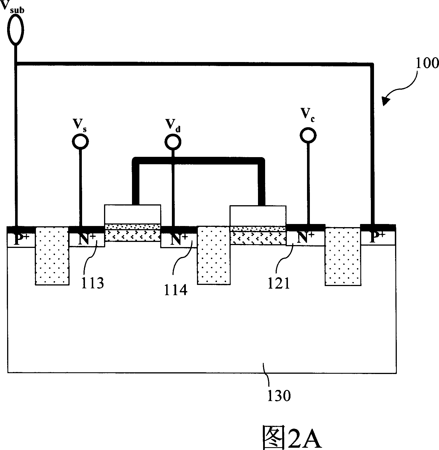
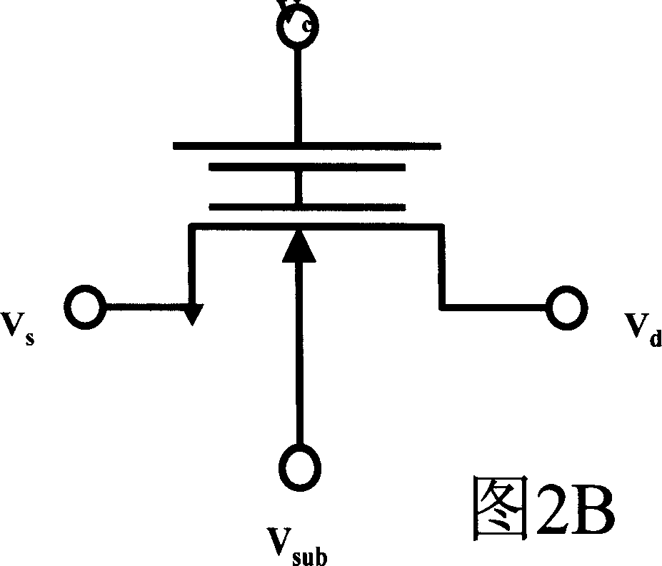
[0136] FIG. 9 is a cross-sectional view of a single-gate non-volatile memory structure provided by a fifth embodiment of the present invention.

[0137] The single-gate non-volatile memory structure 500 includes an NMOS transistor 510 and an N-type capacitor structure 520 in a P-type well 517, and the P-type well 517 is disposed on an N-type semiconductor substrate 530; and the first conductive gate of the NMOS transistor 510 512 and the second conductive gate 523 on top of the N-type capacitor structure 520 are electrically connected and isolated by an isolation material 538 to form a single floating gate 540 structure.

[0138] For the single-ga...


PUM


Abstract

The non-volatile memory includes transistor and capacitance structure embedded in substrate of semiconductor. The transistor includes first electric gate electrode, first dielectric layer, and first ion adulteration area. The capacitance structure includes second electric gate electrode, second dielectric layer, and second ion adulteration area. The first electric gate electrode and the second electric gate electrode are connected each other in electrically to form single suspended jointed gate electrode of memory cell. Using reversal bias, the memory cell can carry out writing, erasing, and reading operations. When operation on insulated trap area, applying positive, negative voltages to drain electrode, gate electrode and silicon substrate or trap area, the method generates inverse layer to reduce absolute voltage and area of boost up circuit so as to lower current consumption.

Description

technical field [0001] The present invention relates to a non-volatile memory (Non-Volatile Memory) and its operating method, in particular to a single-gate non-volatile memory capable of writing and erasing at low voltage and low current consumption and its operation method. How to do it. Background technique [0002] Press, complementary metal oxide semiconductor (Complementary Metal Oxide Semiconductor, CMOS) manufacturing process technology has become a common manufacturing method of application specific integrated circuit (ASIC). With the development of computer information products today, Electronically Erasable Programmable Read Only Memory (EEPROM) has the function of electrically writing and erasing data due to its non-volatile memory function, and after the power is turned off Data will not disappear, so it is widely used in electronic products. [0003] Non-volatile memory is programmable to store charge to change the gate voltage of the memory's transistors, or...

Claims


Application Information

Patent Timeline
Patent Type & Authority Applications(China)
IPC IPC(8): H01L27/115H01L21/8247G11C16/02H01L27/11521
Inventor 林信章黄文谦杨明苍张浩诚吴政颖
Owner YIELD MICROELECTRONICS CORP
Why Eureka
Try Eureka