Low disturbance single grid non-volatile memory and operation approach thereof

A non-volatile, method of operation technology, applied in static memory, read-only memory, information storage, etc., can solve the problems of increasing the cost of boosting area, consuming large current, increasing production cost, etc. effect of speed improvement

Inactive Publication Date: 2008-02-06
YIELD MICROELECTRONICS CORP
View PDF0 Cites 3 Cited by
  • Summary
  • Abstract
  • Description
  • Claims
  • Application Information

AI Technical Summary

Problems solved by technology

Therefore, in the structure of the existing non-volatile memory, the operating voltage often exceeds 10 volts, which not only increases the cost due to the boosted area, but also needs to consume a large amount of current to achieve the purpose of boosting the operation. Moreover, advanced The production of non-volatile memory by the manufacturing process often needs to add a lot of manufacturing processes, which not only increases the difficulty of manufacturing, but also increases the production cost, especially for embedded products; therefore, the current advanced manufacturing processes are all is developing towards low voltage

Method used


Image

  • Low disturbance single grid non-volatile memory and operation approach thereof
  • Low disturbance single grid non-volatile memory and operation approach thereof
  • Low disturbance single grid non-volatile memory and operation approach thereof

Examples


Embodiment 5

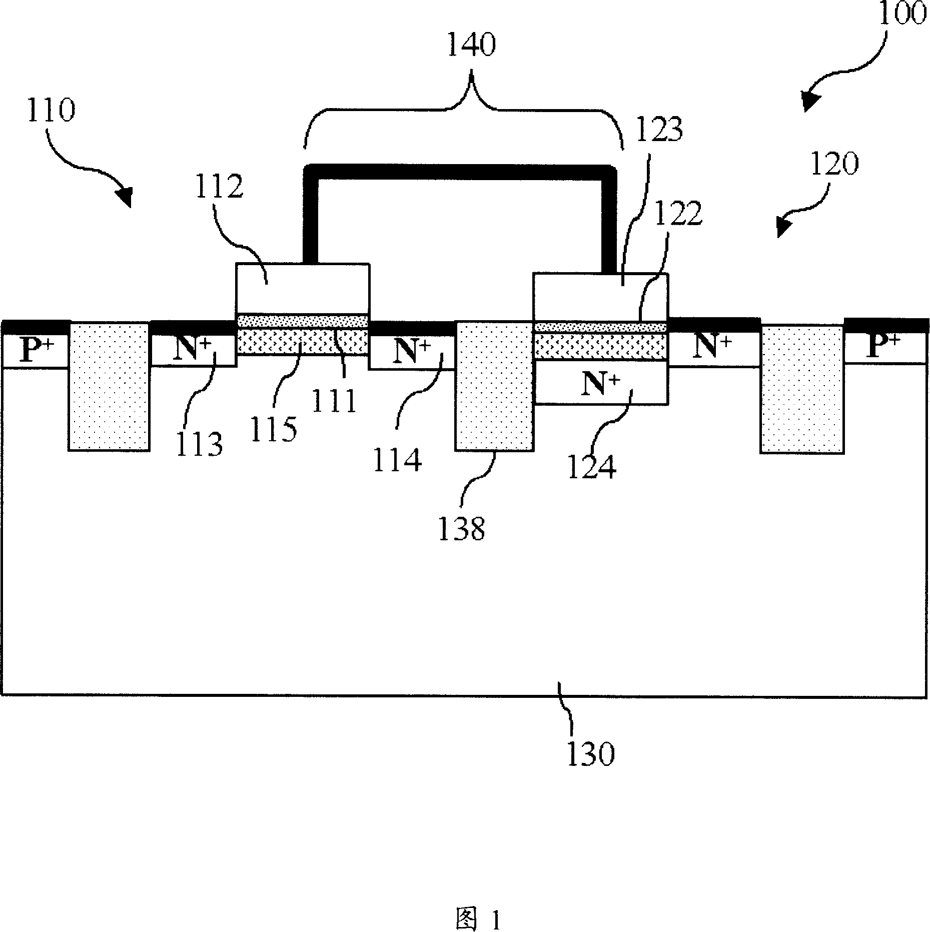
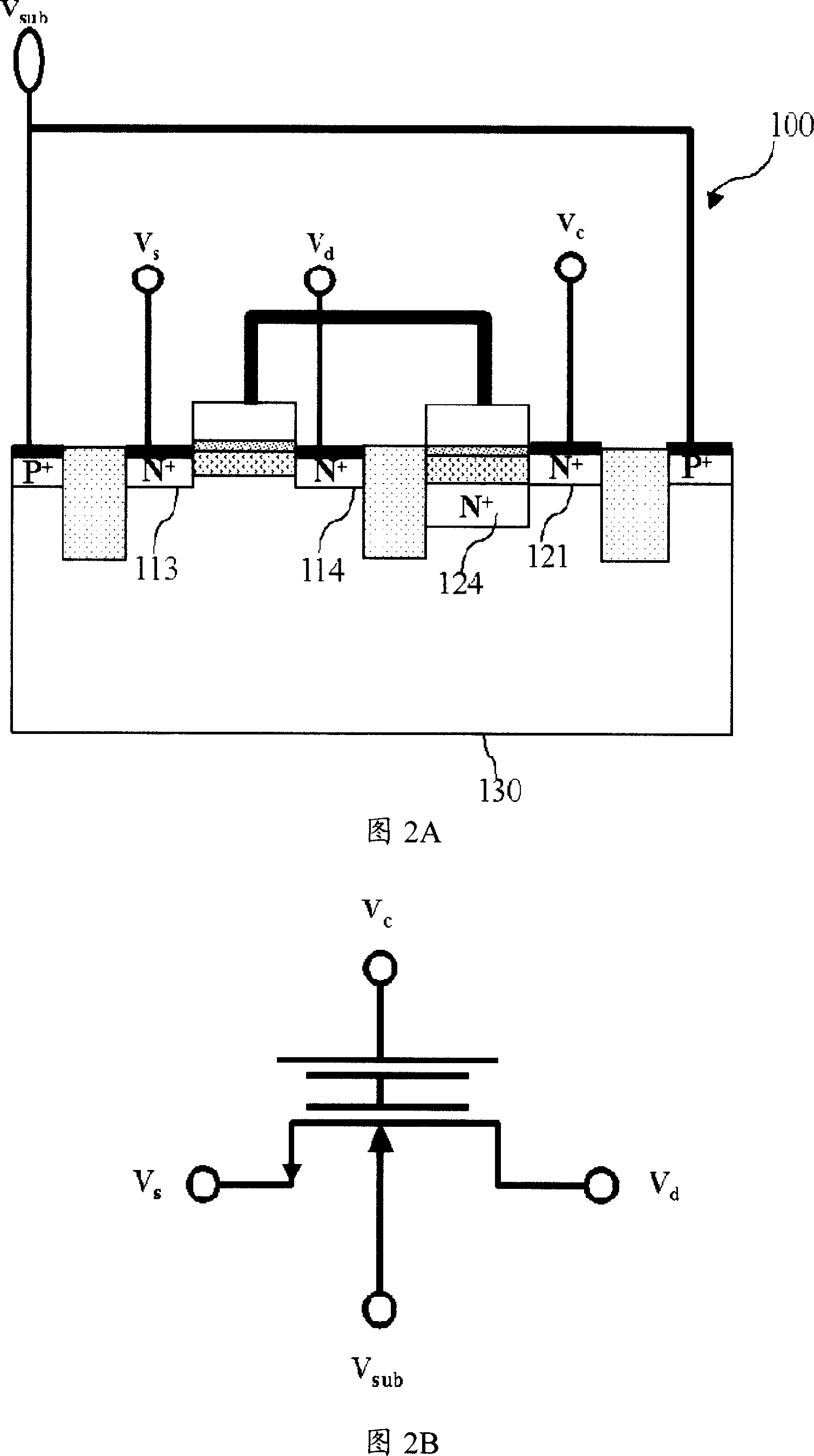
[0143] In addition, the present invention also provides a fifth embodiment, which uses a negative voltage applied to the P-type well, so that the absolute voltage of the drain or gate becomes smaller (less than 5V) during programming and erasing, so as to achieve low voltage and low current consumption operating effect.

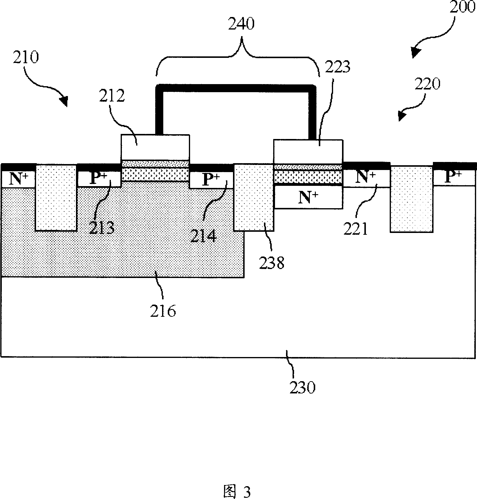
[0144] FIG. 9 is a cross-sectional view of a single-gate nonvolatile memory structure provided by Embodiment 5 of the present invention.

[0145] The low-interference single-gate non-volatile memory structure 500 includes an NMOS transistor 510 and an N-type capacitor structure 520 in a P-type well 517, wherein a second ion is formed under the dielectric layer of the N-type capacitor structure 520. The doped region buried layer 524, the second ion-doped region buried layer 524 is adjacent to the P-type well 517, and the above-mentioned P-type well 517 is arranged on the N-type semiconductor substrate 530; and the first conductive gate of the NMOS transistor 5...


PUM


Abstract

The present invention provides a low interference single gate non-volatile memory and the operation method therein, which embeds a transistor and a capacitance structure in a semiconductor base; the conductive gates in the transistor and in the capacitance structure are electrically interconnected to form a single float-connection gate of a memory cell; and a structure of an ion doping zone burying layer is formed between the dielectric layer and the semiconductor base in the capacitance structure, which is for reducing the interference to the capacitance structure from the outside and can control the initial critical voltage; moreover, the single gate memory cell can perform the operations such as writing, erasing and reading by applying converse bias voltages, and cooperate the operations in the isolation well at the same time; by applying positive and negative voltages on the striking, gate and silicon base or the well, the present inventiongenerates a reversed layer to reduce the absolute voltage and decrease the area of booster circuit, reaching the aim of reducing the current consumption.

Description

technical field [0001] The present invention relates to a non-volatile memory (Non-Volatile Memory) and its operating method, in particular to a low-interference single-gate non-volatile memory that can be written and erased with low voltage and low consumption current Memory and its method of operation. Background technique [0002] At present, the complementary metal oxide semiconductor (Complementary Metal Oxide Semiconductor, CMOS) manufacturing process has become a common manufacturing method for application specific integrated circuits (ASIC). Today, with the development of computer information products, Electronically Erasable Programmable Read Only Memory (Electrically Erasable Programmable Read Only Memory, EEPROM) has the function of electrically writing and erasing data as a non-volatile memory, and after the power is turned off Data will not disappear, so it is widely used in electronic products. [0003] Among them, the non-volatile memory is programmable, and...

Claims


Application Information

Patent Timeline
IPC IPC(8): H01L27/115G11C16/02
Inventor 林信章黄文谦杨明苍张浩诚吴政颖
Owner YIELD MICROELECTRONICS CORP
Why Eureka
Try Eureka