Method for Treating a Cathode Panel, Cold Cathode Field Emission Display Device, and Method for Producing the Same

a display device and cathode field technology, applied in the field of treating a cathode panel and cold cathode field emission display device, can solve the problems of disadvantageous recognition of the emitter area emitting electrons as luminescent spots, and difficulty in producing uniform electron emitters b>15

Inactive Publication Date: 2008-01-17
SONY CORP
View PDF6 Cites 20 Cited by
  • Summary
  • Abstract
  • Description
  • Claims
  • Application Information

AI Technical Summary

Benefits of technology

[0104] A portion of the electron emitter areas in which discharge was produced is separated from a portion of the electron emitter areas in which no discharge was produced. Therefore, there can be provided a cathode panel which is advantageous not only in that it is free of an electron emitter area recognized as a l...

Problems solved by technology

By the way, generally, it is difficult to produce uniform electron emitters 15, especially electron emitters having uniform tip portions.
However, even in the display device having a voltage equal or close to the cut-off volta...

Method used


Image

  • Method for Treating a Cathode Panel, Cold Cathode Field Emission Display Device, and Method for Producing the Same
  • Method for Treating a Cathode Panel, Cold Cathode Field Emission Display Device, and Method for Producing the Same
  • Method for Treating a Cathode Panel, Cold Cathode Field Emission Display Device, and Method for Producing the Same

Examples


example 1

[0121] Example 1 is directed to the method for treating a cathode panel of the present invention, a cold cathode field emission display device (hereinafter, referred to simply as “display device”), and a method for producing the same.

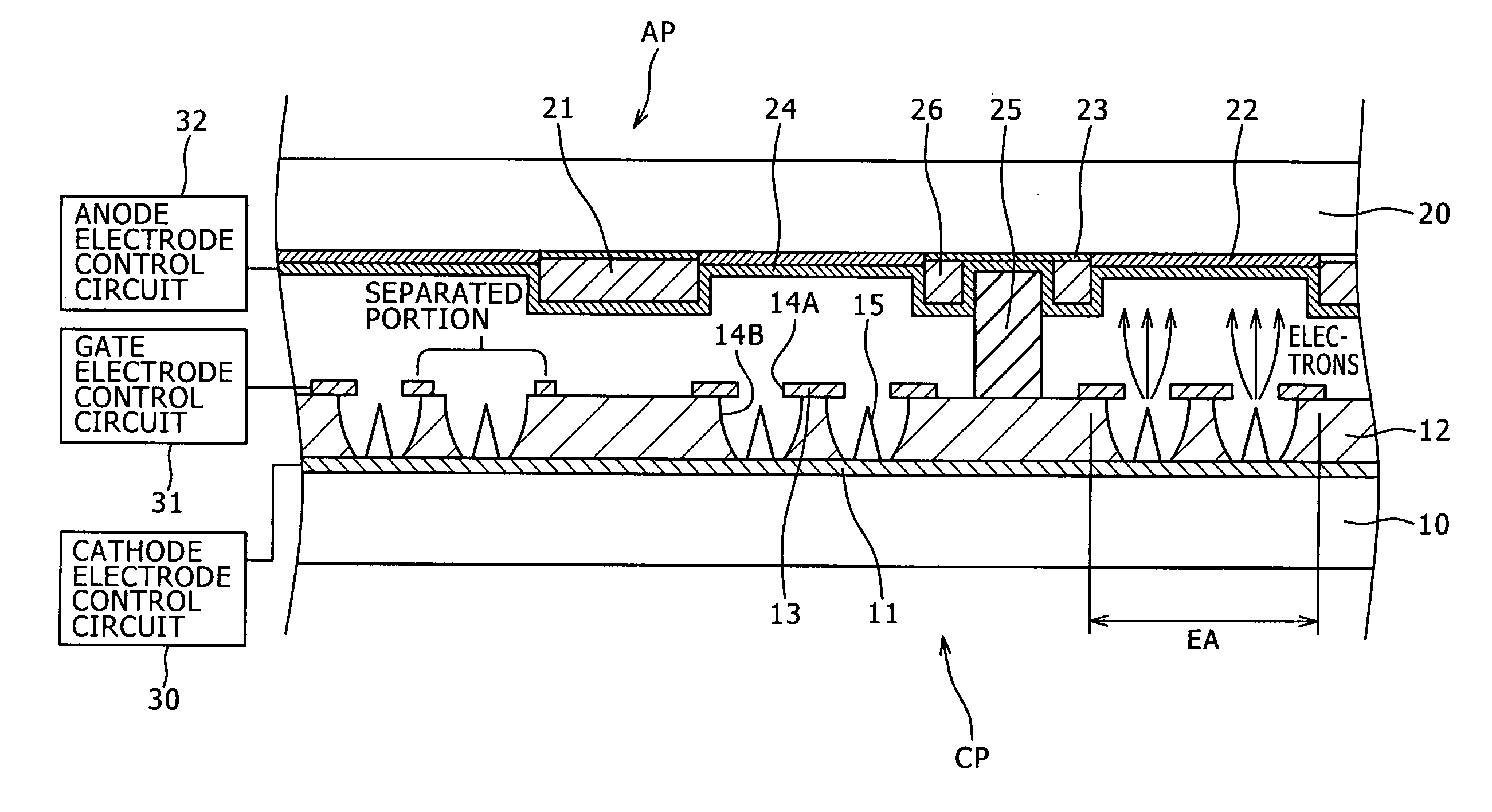
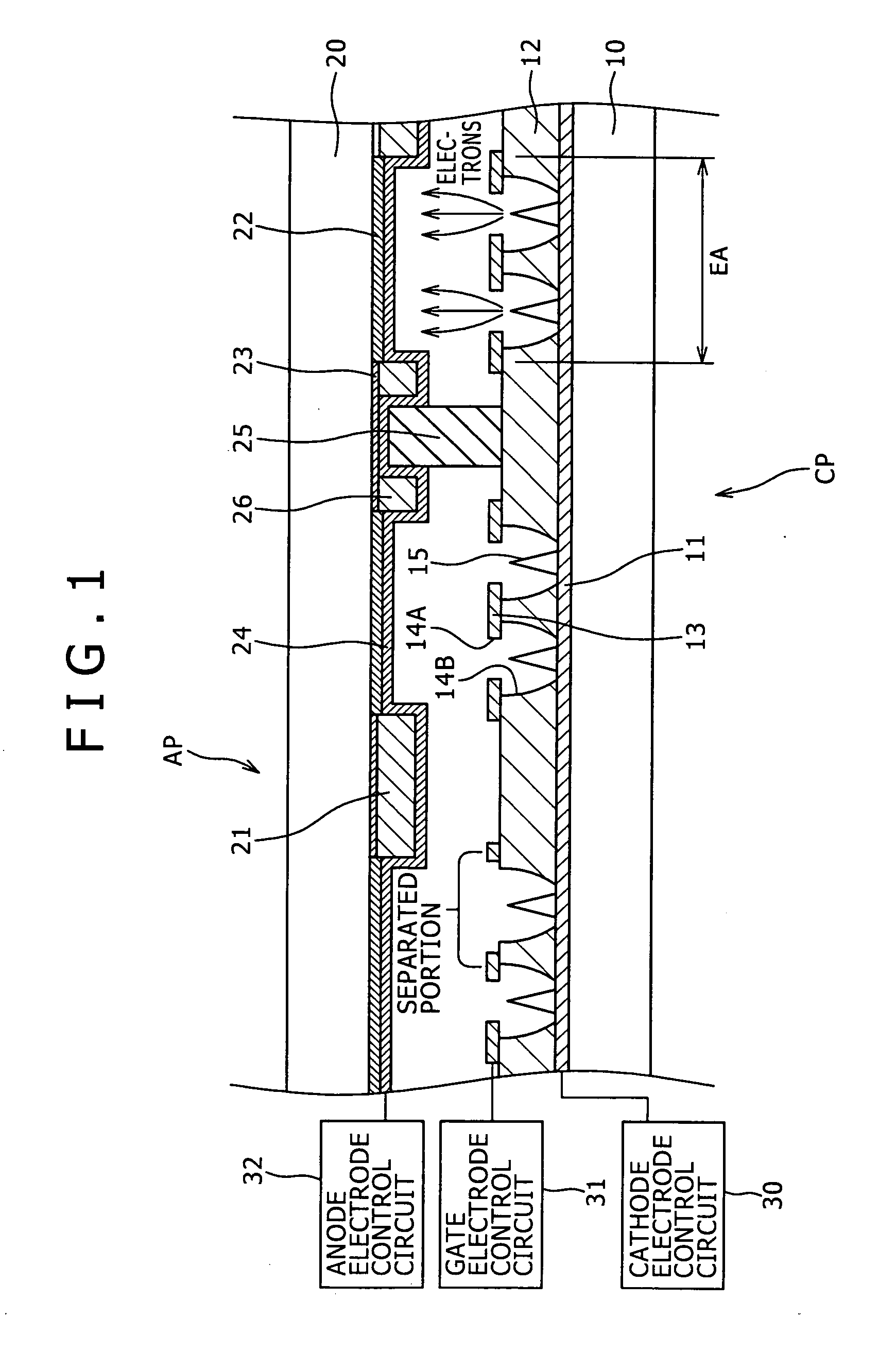
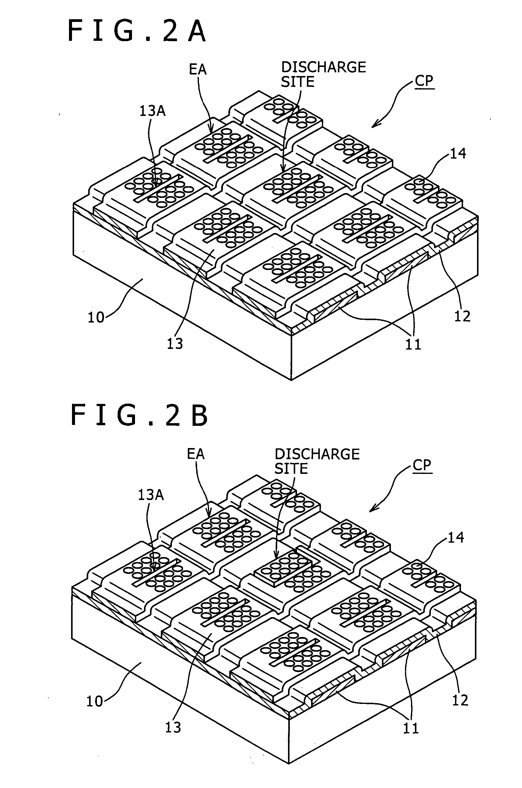
[0122] A diagrammatic fragmentary end view of the display device in Example 1 is shown in FIG. 1, and partial, diagrammatic perspective views of a cathode panel are shown in FIGS. 2A and 2B. Further, examples of arrangements of the fluorescent regions and others are shown in diagrammatic partial top views of FIGS. 3 to 8. The arrangement of the fluorescent regions and others in the anode panel AP shown in the diagrammatic fragmentary end view of FIG. 1 is shown in FIG. 4 or FIG. 6. In FIGS. 3 to 8, no anode electrode is shown. The diagrammatic perspective view of the anode panel AP in Example 1 is similar to that of the anode panel AP shown in FIG. 15.

[0123] The display device in Example 1 includes a cathode panel CP and an anode panel AP joined toget...


PUM


Abstract

A method for treating a cathode panel, which is used for obtaining a cathode panel free of an electron emitter area recognized as a luminescent spot when the cold cathode field emission display device collectively makes the darkest display. A method for treating a cathode panel (CP) having a plurality of electron emitter areas arrayed in a two-dimensional matrix form for use in producing a cold cathode field emission display device having a predetermined internal pressure P0, wherein the method includes: (A) placing the cathode panel (CP) in a treatment chamber (100) having a predetermined internal pressure P1 (where P1>P0, preferably P1>>P0); and then (B) applying an inspection voltage (VINS) to each electron emitter area such that each electron emitter area emits electrons, causing discharge in an electron emitter area having an electron emission amount larger than that of another electron emitter area.

Description

TECHNICAL FIELD [0001] The present invention relates to a method for treating a cathode panel constituting a cold cathode field emission display device, a method for producing a cold cathode field emission display device using the method for treating a cathode panel, and a cold cathode field emission display device obtained by the method for producing a cold cathode field emission display device. BACKGROUND ART [0002] As image display devices which will possibly replace cathode-ray tubes (CRTs) currently widely spread, plane-type (flat panel type) display devices are vigorously studied. Examples of the plane-type display devices include a liquid crystal display (LCD), an electroluminescence display (ELD), and a plasma display (PDP). In addition, a cold cathode field emission display device in which a solid material can emit electrons into a vacuum without using thermal excitation, i.e., a so-called field emission display (FED) has been proposed, and has attracted attention since it ...

Claims


Application Information

Patent Timeline
IPC IPC(8): H01J1/62F23Q23/08H01J9/04H01J9/02H01J31/12H01J9/42
CPCH01J9/025H01J31/127H01J9/42
Inventor NEGISHI, EISUKE
Owner SONY CORP
Why Eureka
Try Eureka