
Data Latch

Active Publication Date: 2008-01-17
NXP USA INC
View PDF7 Cites 3 Cited by
  • Summary
  • Abstract
  • Description
  • Claims
  • Application Information

AI Technical Summary

Problems solved by technology

In multi-gigahertz processor designs, the setup and launch delay through latches have become a significant portion of the cycle time.
The sum of the setup time and launch delay of the latch, if large, exacerbates the delay in the critical timing paths.
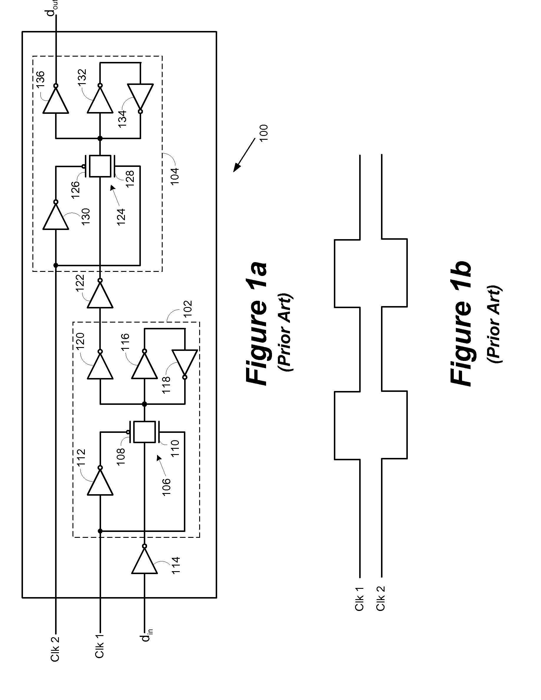
While the setup and hold time for master-slave latches has been acceptable in many prior art processors, they present design problems in processors with multi-gigahertz speeds.
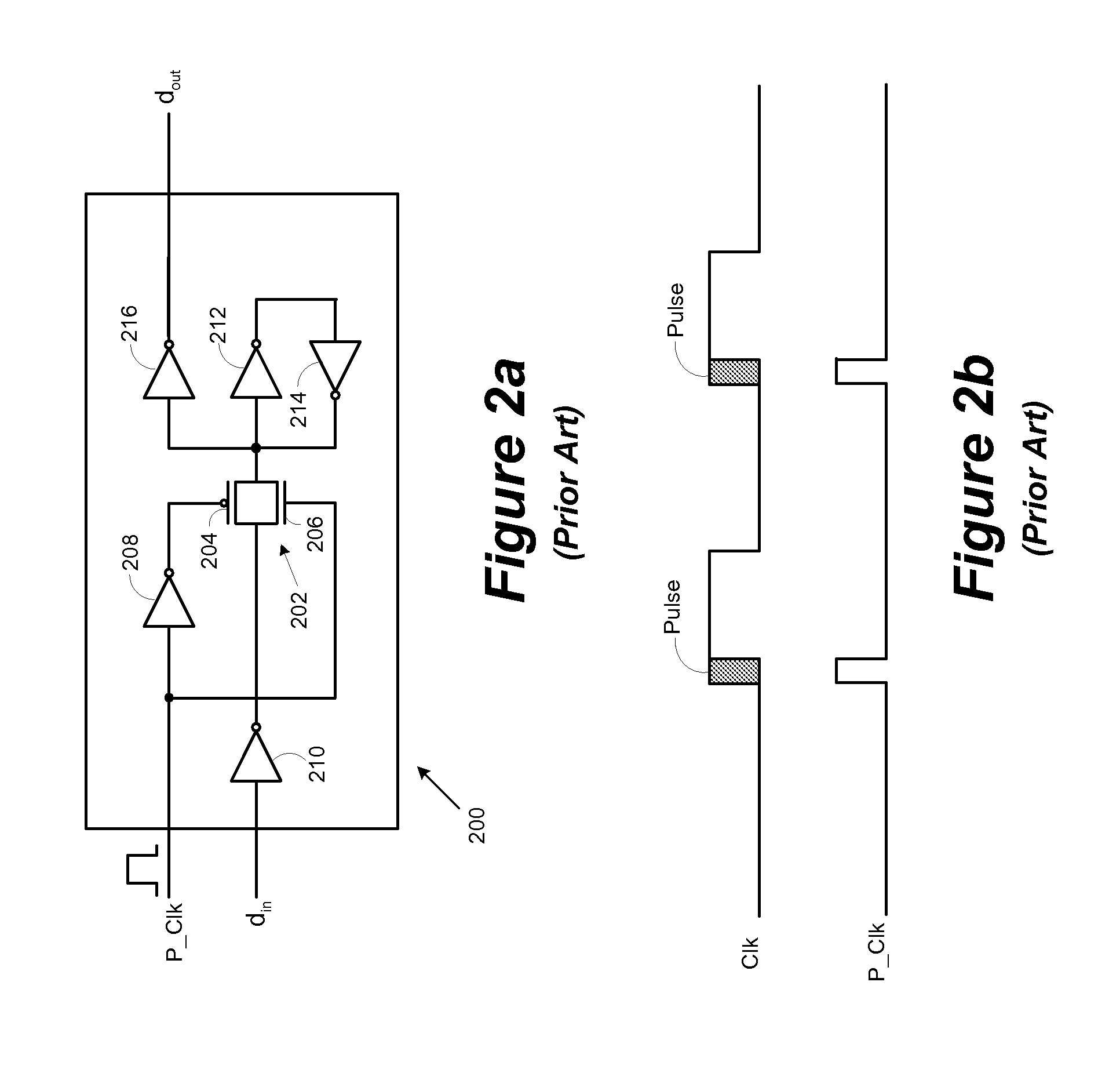
The pulse latch, however, requires a controlled pulse clock and the pulse generation circuit is very sensitive to process variation, which can affect the robustness of the pulse latch.
Another problem with prior art pulse generation circuitry is that a single pulse generator is generally used to generate pulses for an entire datapath.
The solution for one process and feature size, however, does not readily translate to other feature sizes.

Method used


Image

  • Data Latch
  • Data Latch
  • Data Latch

Examples


Embodiment Construction

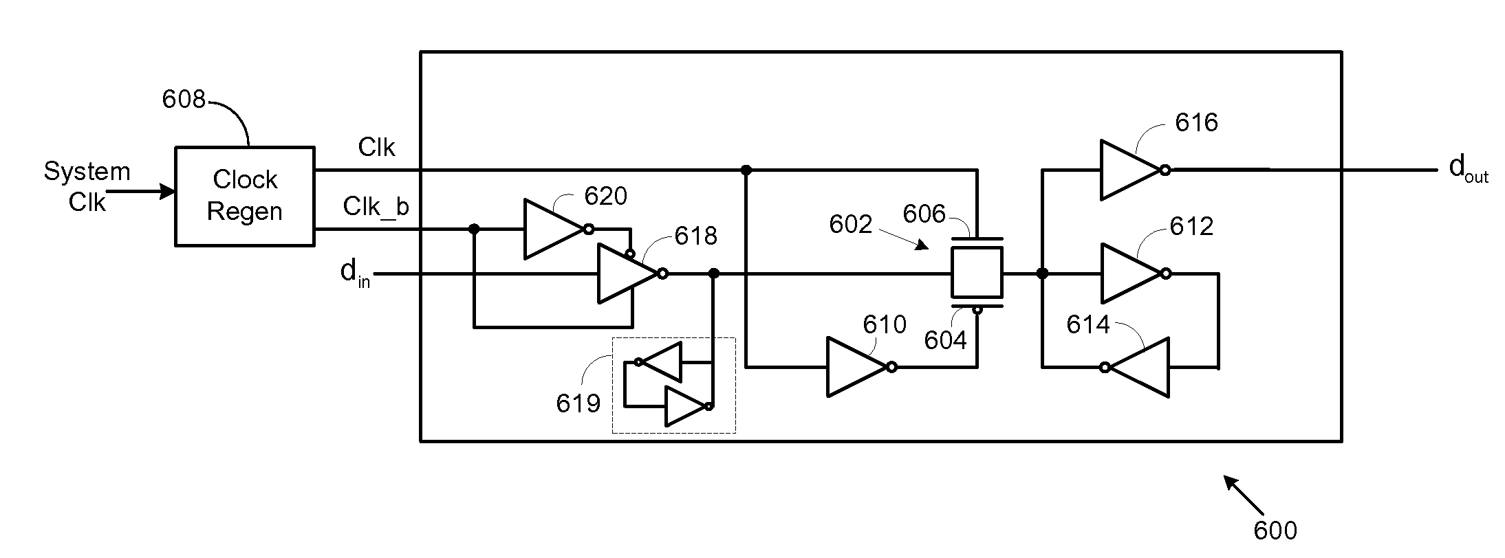
[0030]Embodiments of logic circuitry are described for generating and utilizing a plurality of clock signals to minimize the propagation time for data transferred by latches in a datapath. The disclosed circuitry can be used to minimize the setup time and launch delay through the latches that are becoming a significant portion of the cycle time in modern processors. Various illustrative embodiments of the present invention will now be described in detail with reference to the accompanying figures. While various details are set forth in the following description, it will be appreciated that the present invention may be practiced without these specific details, and that numerous implementation-specific decisions may be made to the invention described herein to achieve the device designer's specific goals, such as compliance with process technology or design-related constraints, which will vary from one implementation to another. While such a development effort might be complex and tim...


PUM


Abstract

The present invention provides a latch circuit that is operable to generate a pulse from first and second clock signals to allow gates in a datapath to propagate data with minimal latency. The first clock signal is a version of the system clock and the second control signal is a time-shifted, inverted version of the system clock signal. Each of the individual latches in a datapath comprises data propagation logic. In one embodiment of the invention, the data propagation logic uses the first and second clock signals to generate an “implicit” pulse. In another embodiment of the invention, the data propagation logic uses the first and second clock signals to generate an “explicit” pulse. The implicit and explicit pulses are used to control the transmission gate of the latch to provide propagation of data through the latch with minimal latency.

Description

BACKGROUND OF THE INVENTION[0001]1. Field of the Invention[0002]The present invention relates in general to the field of information processing, and more specifically to a system and method for efficiently transferring data using latches in a datapath.[0003]2. Description of the Related Art[0004]Latches are one of the most common digital circuits used in modern data processing devices. In multi-gigahertz processor designs, the setup and launch delay through latches have become a significant portion of the cycle time. The sum of the setup time and launch delay of the latch, if large, exacerbates the delay in the critical timing paths. An optimal latch design would have a minimum combined sum of setup time (din to clock) and launch (clock to dout).[0005]Master-slave latches are commonly used to propagate data through various datapaths within a data processing system. Such latches typically use multiple clocks to enable the master and the slave portions of the latch to receive data inp...

Claims


Application Information

Patent Timeline
IPC IPC(8): H03K3/289
CPCH03K3/356156H03K3/0375
Inventor RAMARAJU, RAVINDRARAJASHOK, AMBICACROXTON, CODY B.IPPOLITO, PETER M.KENKARE, PRASHANT U.
Owner NXP USA INC
Learn More