Liquid crystal display device, method of driving the same, and method of manufacturing the same
a liquid crystal display and liquid crystal module technology, applied in the direction of optics, instruments, electrical devices, etc., can solve the problem of difficult constant maintenance of the potential of the pixel electrode during the one fram
- Summary
- Abstract
- Description
- Claims
- Application Information
AI Technical Summary
Problems solved by technology
Method used
Image
Examples
embodiment 1
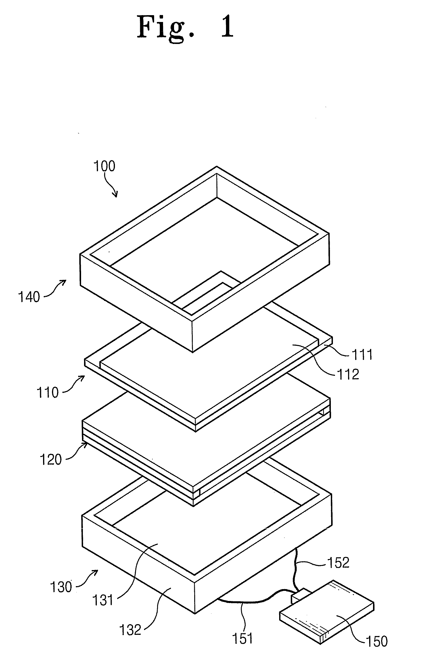
[0037]FIG. 1 is an exploded perspective view showing an exemplary embodiment of a liquid crystal display according to the present invention.
[0038] Referring to FIG. 1, a liquid crystal display (“LCD”) 100 includes a liquid crystal module 110, a backlight unit 120, a container 130 which contains the liquid crystal module 110 and the backlight unit 120, and a top chassis 140.
[0039] The liquid crystal module 110 includes a thin film transistor ( “TFT”) substrate 111, an opposite substrate 112, which faces the TFT substrate 111, and a liquid crystal layer (not shown) arranged between the TFT substrate 111 and the opposite substrate 112. In one exemplary embodiment the opposite substrate 112 comprises a color filter substrate.
[0040] Exemplary embodiments of the present invention are not limited to the use of the TFT substrate 111, but can employ various types of substrates with thin film transistors and electrodes formed thereon. In one exemplary embodiment the liquid crystal module e...
embodiment 2
[0079] Another exemplary embodiment employs a structure including a storage capacitor common line SC shared between neighboring pixels in the liquid crystal module 110.
[0080]FIG. 9 is an equivalent circuit diagram showing another exemplary embodiment of a pixel module 110a according to the present invention.
[0081] Referring to FIG. 9, the exemplary embodiment of a pixel module 110a of the liquid crystal module 110 according to the present invention has a plurality of pixels 200 arranged in a matrix pattern. According to the current exemplary embodiment, the pixel module 110a has m×n pixels 200 arranged therein, wherein m and n represent natural numbers. A (k, i)th pixel 200 is connected to a source line Si, a first gate line Gk, and a second gate line Gkcont. According to the current exemplary embodiment, a storage capacitor common line SC is shared between neighboring pixels. Thus, in addition to the benefits obtained by the first embodiment of the present invention, the number o...
embodiment 3
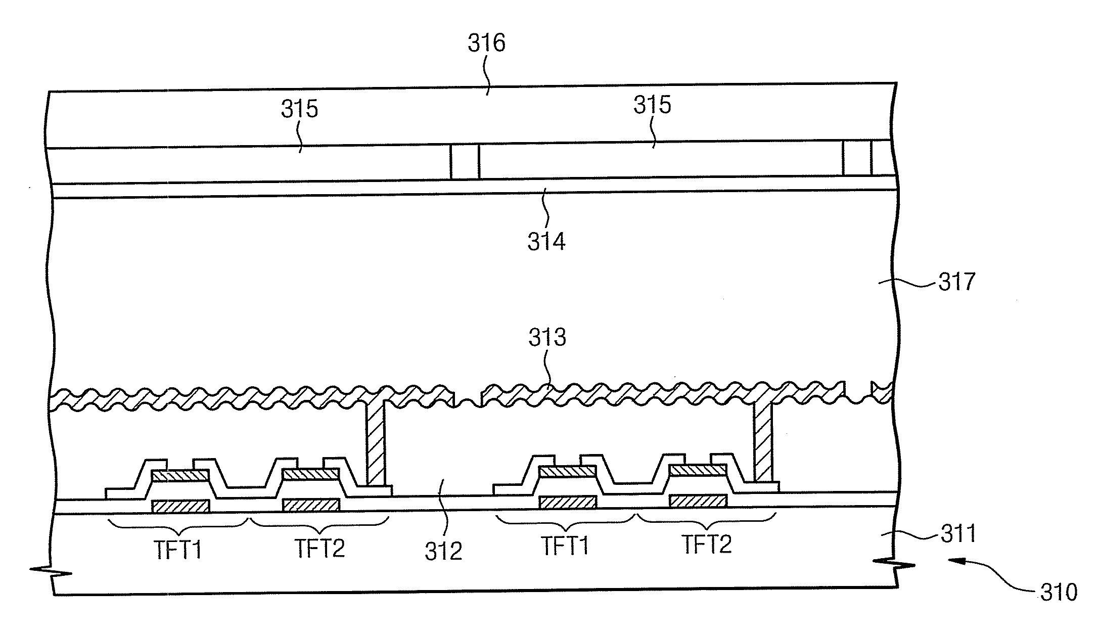
[0082] According to another exemplary embodiment, a first thin film transistor TFT1 and a second thin film transistor TFT2 constituting a pixel module 110a of a liquid crystal module 110 according to the present invention include amorphous silicon thin film transistors.
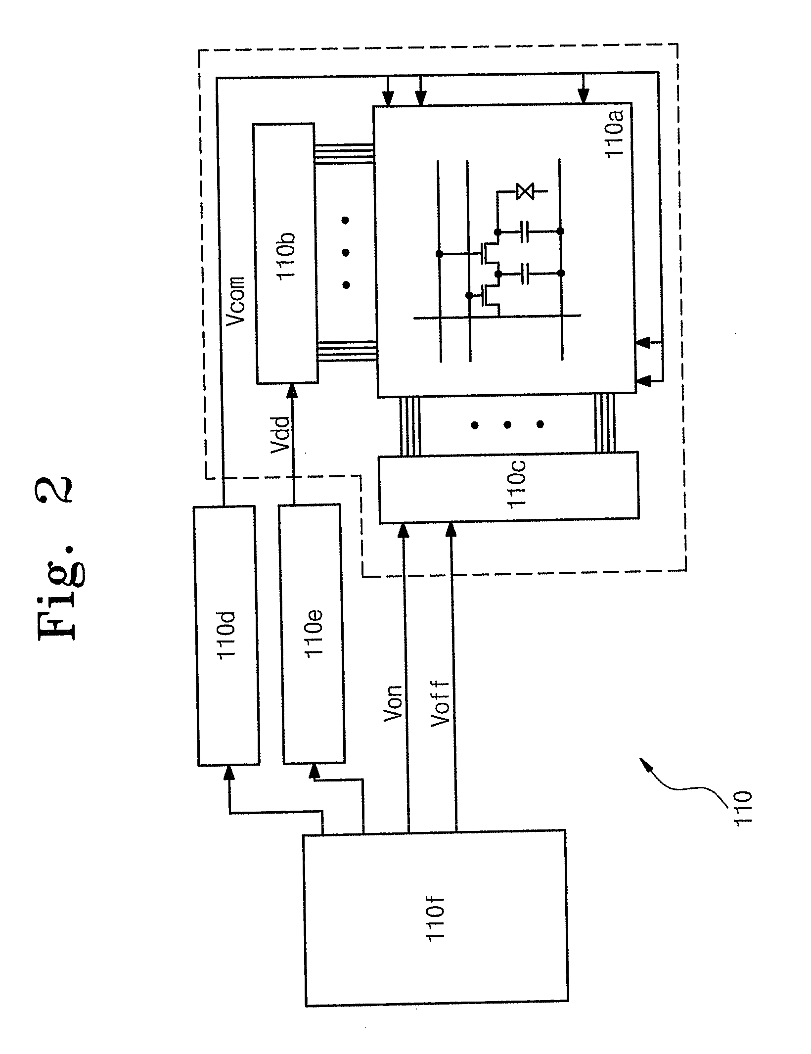
[0083] A liquid crystal module 110 according to the current exemplary embodiment has the same functional block diagram as the liquid crystal module 110 shown in FIG. 2. According to the current exemplary embodiment, the first thin film transistor TFT1 and the second thin film transistor TFT2 in a pixel 200 of the pixel module 110a include amorphous silicon thin film transistors, and a data line driving circuit 110b, a gate line driving circuit 110c, a common voltage Vcom generator 110d, a gamma voltage generator 110e, and a DC / DC converter 110f are constructed using integrated circuits on IC chips.
PUM
 Abstract
Description
Claims
Application Information


