Operation method of nonvolatile memory device induced by pulse voltage

a nonvolatile memory and pulse voltage technology, applied in the direction of information storage, static storage, digital storage, etc., can solve the problems of difficult to fabricate a dram cell having a higher throughput and the capacitor process, and achieve the effect of low curren

Inactive Publication Date: 2008-01-17
SAMSUNG ELECTRONICS CO LTD
View PDF9 Cites 57 Cited by
  • Summary
  • Abstract
  • Description
  • Claims
  • Application Information

AI Technical Summary

Benefits of technology

[0010] Example embodiments may provide a threshold switching operation method of a nonvolatile memory devi

Problems solved by technology

The smaller a device may be, the more difficult a capacitor process may b

Method used


Image

  • Operation method of nonvolatile memory device induced by pulse voltage
  • Operation method of nonvolatile memory device induced by pulse voltage
  • Operation method of nonvolatile memory device induced by pulse voltage

Examples


Embodiment Construction

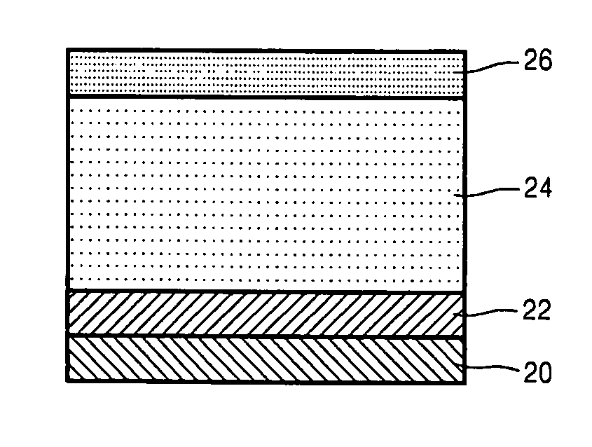
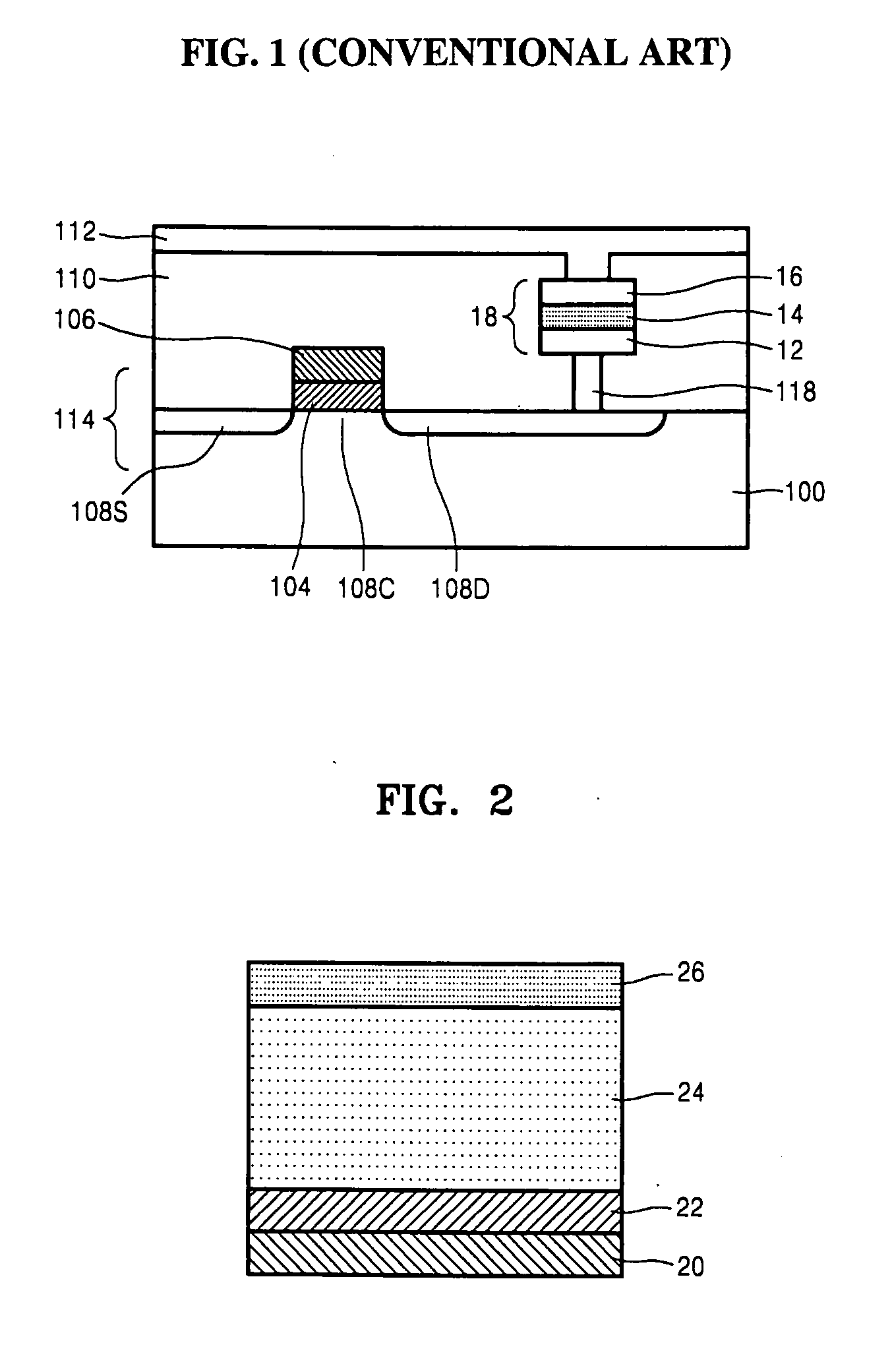
[0033] Example embodiments will now be described more fully hereinafter with reference to the accompanying drawings. Embodiments may, however, be in many different forms and should not be construed as being limited to the example embodiments set forth herein. Rather, these example embodiments are provided so that this disclosure will be thorough and complete, and will fully convey the scope to those skilled in the art. In the drawings, the thicknesses of layers and regions may be exaggerated for clarity.

[0034] It will be understood that when a component is referred to as being “on,”“connected to” or “coupled to” another component, it can be directly on, connected to or coupled to the other component or intervening components may be present. In contrast, when a component is referred to as being “directly on,”“directly connected to” or “directly coupled to” another component, there are no intervening components present. As used herein, the term “and / or” includes any and all combinati...


PUM


Abstract

A threshold switching operation method of a nonvolatile memory device may be provided. In the threshold switching operation method of a nonvolatile memory a pulse voltage may be supplied to a metal oxide layer of the nonvolatile memory device. Accordingly, it may be possible to operate the nonvolatile memory device at a lower voltage with lower threshold switching current.

Description

PRIORITY STATEMENT [0001] This application claims the benefit of priority to Korean Patent Application No. 10-2006-0058096, filed on Jun. 27, 2006, in the Korean Intellectual Property Office, the entire contents of which is incorporated herein in its entirety by reference. BACKGROUND [0002] 1. Field [0003] Example embodiments relate to a method of operating a nonvolatile memory device, and for example, to a method of operating a nonvolatile memory device, in which a metal oxide layer may be formed between a lower electrode and an upper electrode, by supplying pulse voltage to the nonvolatile memory device so that the nonvolatile memory device may manifest switching characteristics, for example, the nonvolatile memory device may operate at a lower voltage with lower threshold current. [0004] 2. Description of Related Art [0005] In a conventional Dynamic Random Access Memory (DRAM) process, a transistor / capacitor may form a unit cell. The smaller a device may be, the more difficult a ...

Claims


Application Information

Patent Timeline
IPC IPC(8): G11C11/21
CPCG11C13/0007G11C2213/32G11C2013/009G11C13/0069G11C13/0038
Inventor KIM, DONG-CHULBAEK, IN-GYUSUH, DONG-SEOKLEE, MYOUNG-JAEAHN, SEUNG-EON
Owner SAMSUNG ELECTRONICS CO LTD
Why Eureka
Try Eureka