Modular design of multiport memory bitcells

a memory bitcell and module design technology, applied in the field of memory devices, can solve the problems of complex design process, further complicated design process, and complex design process of multi-port bitcells, and achieve the effect of reducing the complexity of designing multi-port bitcells and being easy to interconn

Inactive Publication Date: 2008-01-17
AVAGO TECH INT SALES PTE LTD
View PDF4 Cites 14 Cited by
  • Summary
  • Abstract
  • Description
  • Claims
  • Application Information

AI Technical Summary

Benefits of technology

[0011]The present invention provides a system and method for designing and modularly expanding multiport bitcells. A modular design approach is described that reduces the complexity of designing multiport bitcells while complying with DFM rules across various semiconductor fabrication providers. The modular design may be parsed into modules such as read port modules, write port modules, and pull-up modules that may be easily interconnected to build a multiport bitcell. These modules may also be independently sized and assembled to achieve desired read margins, write margins, static noise margins as well as read access times and write times.
[0012]In various embodiments of the present invention, a multiport design layout structure is provided that comprises unidirectional polysilicon in one direction and diffusion segments in the opposite direction. These diffusion segments are not enclosed and do not contain any breaks along a memory array in order to minimize systematic process-induced non-uniformities between the devices in the memory bitcell. As a result of this and other aspects of the invention, modularly designed multiport bitcells are able to maintain compliance with the various DFM rules.
[0013]The bitcell may also be designed with voltage lines positioned to provide shielding between bitlines and or wordlines. This shielding reduces inter-port interference within the bitcell resulting in improved electrical performance.
[0014]In various embodiments of the invention, a multiport bitcell design may use split-gate devices that provide flexibility in adding ports to the cell. A read port may effectively be split into “top” and “bottom” halves with a common wordline connection. As a result, an engineer may adjust the width and / or height of a bitcell and improve the beta ratio for a given width used in the layout. These split-gate devices may also improve area efficiency within the bitcell and increase the read performance of the port without increasing the width of the bitcell.

Problems solved by technology

The design process for multiport bitcells is often complex because of performance and density requirements as well as manufacturability rules imposed by various semiconductor fabrication providers.
These rules often impose significant restrictions on multiport bitcell designs and significantly complicate the design process.
The design process is further complicated because it is often difficult to leverage previous multiport bitcell designs into a new design.
For example, if a designer wanted to expand the number of ports in a bitcell, he / she may be unable to leverage a significant portion of the smaller multiport bitcell in the new design.
As semiconductor fabrication techniques further advance, it is likely that DFM rules may become even more stringent and further complicate the design process.
As a result, the ability to leverage previous bitcell designs when expanding the number ports may become even more difficult.

Method used


Image

  • Modular design of multiport memory bitcells
  • Modular design of multiport memory bitcells
  • Modular design of multiport memory bitcells

Examples


Embodiment Construction

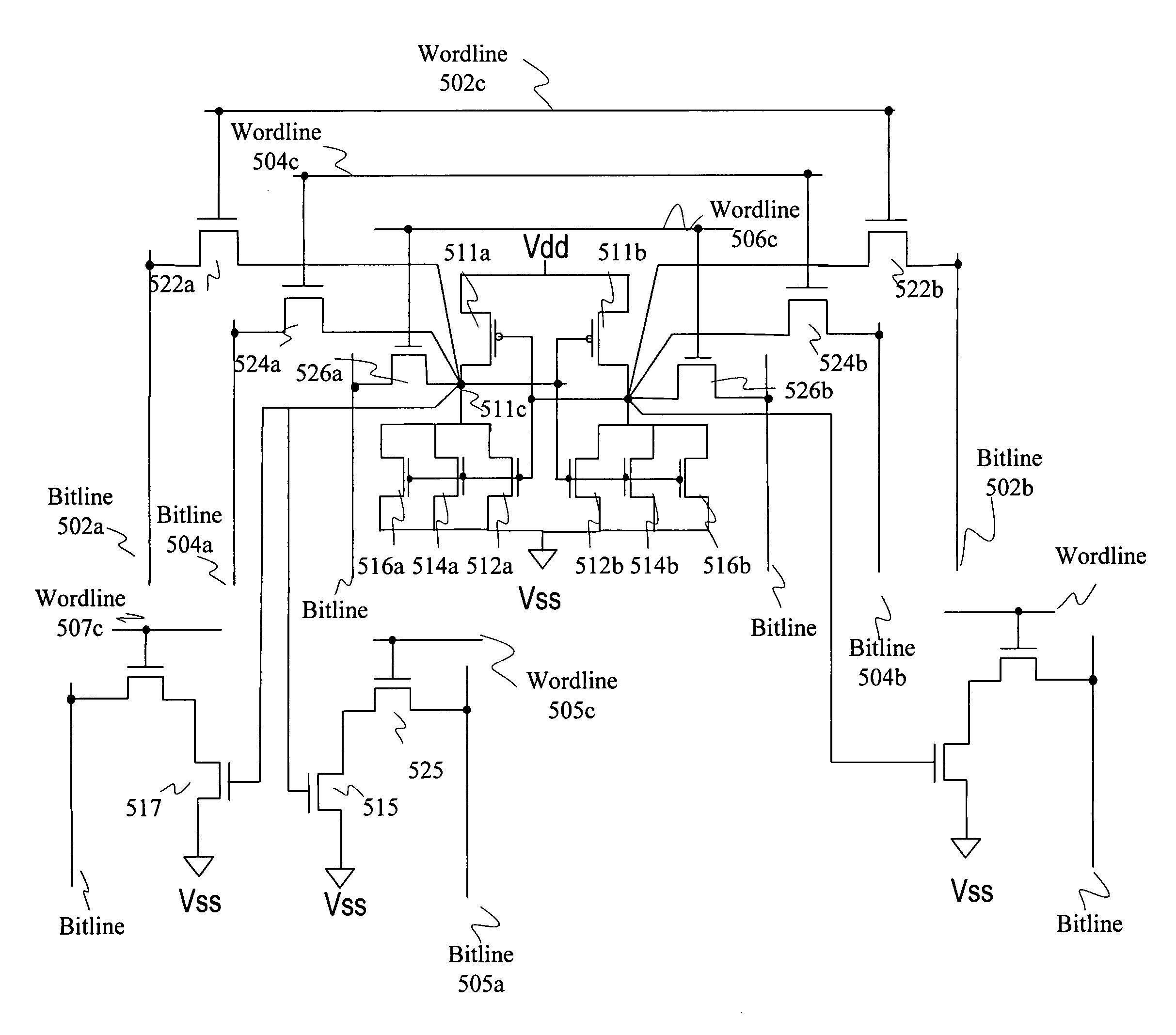
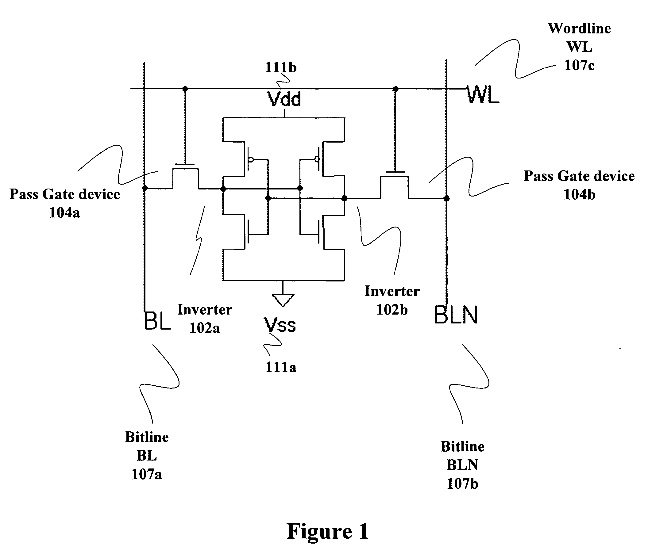
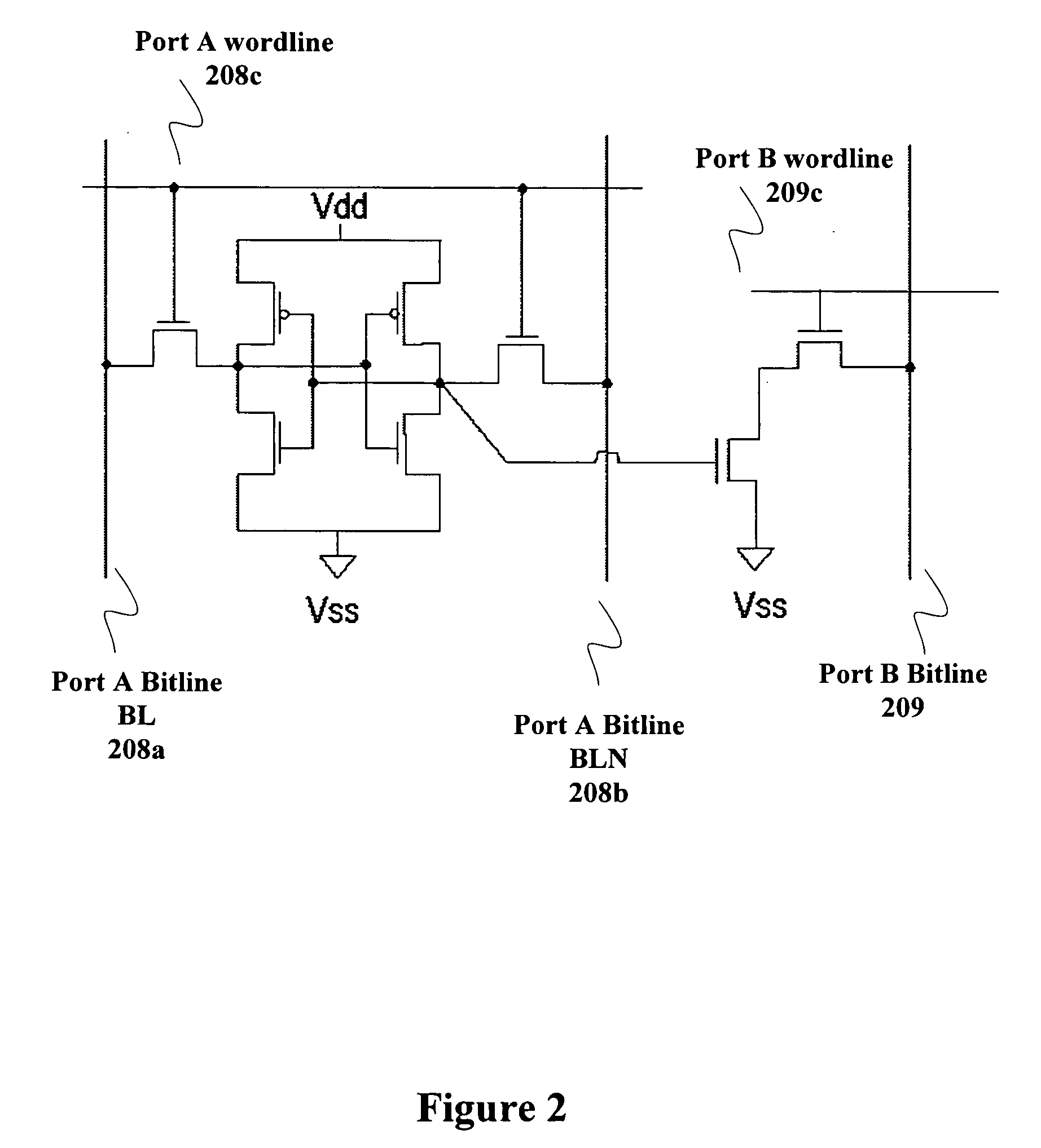
[0028]The present invention provides a system and method for designing and modularly expanding multiport bitcells. A modular design approach is described that reduces the complexity of designing multiport bitcells while complying with DFM rules across various semiconductor fabrication providers. The modular design may be parsed into modules such as read port modules, write port modules, and pull-up modules that may be easily interconnected to build a multiport bitcell. These modules may also be independently sized and assembled to achieve desired read margins, write margins, static noise margins as well as read access times and write times.

[0029]In the following description, for purpose of explanation, specific details are set forth in order to provide an understanding of the invention. It will be apparent, however, to one skilled in the art that the invention may be practiced without these details. One skilled in the art will recognize that embodiments of the present invention, som...


PUM


Abstract

The present invention provides a system and method for designing and modularly expanding multiport bitcells. A modular design approach is described that reduces the complexity of designing multiport bitcells while complying with DFM rules across various semiconductor fabrication providers. The modular design may be parsed into modules such as read port modules, write port modules, and pull-up modules that may be easily interconnected to build a multiport bitcell. These modules may also be independently sized and assembled to achieve desired read margins, write margins, static noise margins as well as read access times and write times.

Description

BACKGROUND[0001]A. Technical Field[0002]The present invention relates generally to memory devices and more particularly, to a modular design and layout of a multiport memory bitcell having an expandable number of access ports.[0003]B. Background of the Invention[0004]Memory is an essential part of any computation system. A typical memory system may be viewed as a collection of sequential locations, each with a unique address and capable of storing information. Memories are broadly classified based on their functionality as Read Only Memory (“ROM”) or Random Access Memory (“RAM”). Random access memories are further differentiated in static (“SRAM”) or dynamic (“DRAM”) RAM, depending on how the data is stored in the memory bitcell. Memory bitcells can have one or more ports to access stored data. Memory bitcells with multiple ports are typically referred to as multiport memory bitcells. A memory that uses such multiport memory bitcells enables multiple system elements to directly and ...

Claims


Application Information

Patent Timeline
Patent Type & Authority Applications(United States)
IPC IPC(8): G11C7/10
CPCG11C8/16H01L27/1104H01L27/11G11C11/412H10B10/00H10B10/12
Inventor VENKATRAMAN, RAMNATHCASTAGNETTI, RUGGERORAMESH, SUBRAMANIAN
Owner AVAGO TECH INT SALES PTE LTD
Why Eureka
Try Eureka