Method For The Simultaneous Double-Side Grinding Of A Plurality Of Semiconductor Wafers, And Semiconductor Wafer Having Outstanding Flatness

a technology of semiconductor wafers and double-side grinding, which is applied in the direction of grinding machine components, manufacturing tools, lapping machines, etc., can solve the problems of affecting the performance of the machine, the uneven thickness the disadvantages of convex thickness profiles of the semiconductor wafer, so as to prevent the edge from rolling off and the line width is small.

Active Publication Date: 2008-01-17
PETER WOLTERS GMBH
View PDF16 Cites 41 Cited by
  • Summary
  • Abstract
  • Description
  • Claims
  • Application Information

AI Technical Summary

Benefits of technology

[0017]It is an object of the present invention, therefore, to provide semiconductor wafers which, on account of their geometry, are also suitable for producing electronic components with very small linewidths (“design rules”). A further object was to prevent edge roll-off from arising during the production of semiconductor wafers, and a yet further object was to avoid other geometrical faults such as a thickness maximum in the center of the semiconductor wafer associated with a continuously decreasing thickness toward the edge of the wafer or a local thickness minimum in the center of the semiconductor wafer. These and other objects, separately or together, are surprisingly met by the process of the invention.

Problems solved by technology

It has been found, however, that the semiconductor wafers machined by this method have a series of defects, with the result that the wafers are unsuitable for particularly demanding applications.
It has been shown, for example, that generally semiconductor wafers are produced with a disadvantageous convex thickness profile and a pronounced edge roll-off.
The semiconductor wafers also often have irregular undulations in their thickness profile and also a rough surface with a large damage depth.
It is virtually impossible or possible only with high outlay to convert convex semiconductor wafers into the desired plane-parallel target form by means of the customary chemical and chemomechanical subsequent machining.
The remaining convexity and edge roll-off lead to incorrect exposures during photolithographic device patterning and hence to the failure of the components.
Semiconductor wafers of this type are therefore unsuitable for demanding applications.

Method used


Image

  • Method For The Simultaneous Double-Side Grinding Of A Plurality Of Semiconductor Wafers, And Semiconductor Wafer Having Outstanding Flatness
  • Method For The Simultaneous Double-Side Grinding Of A Plurality Of Semiconductor Wafers, And Semiconductor Wafer Having Outstanding Flatness
  • Method For The Simultaneous Double-Side Grinding Of A Plurality Of Semiconductor Wafers, And Semiconductor Wafer Having Outstanding Flatness

Examples


example 1

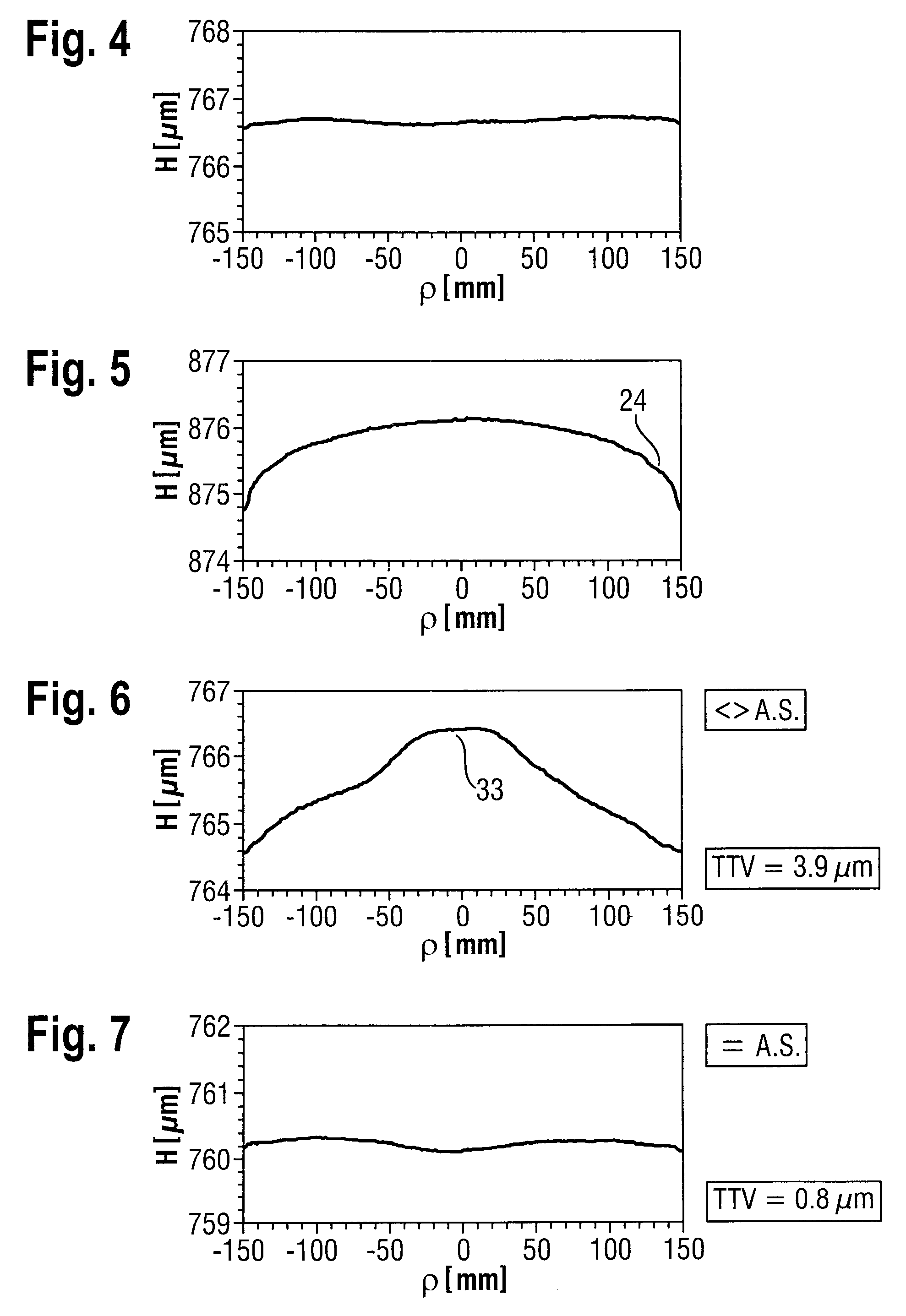
[0184]FIG. 4 shows the thickness profile of a semiconductor wafer made of monocrystalline silicon having a diameter of 300 mm which was obtained by machining by a method according to the invention having all the features of the first, second, third, fourth and fifth inventive methods. The thickness profile was determined by averaging 4 diametrically proceeding individual measurements at 0°, 45°, 90° and 135° relative to the orientation characteristic notch of the semiconductor wafer. The thickness variation over the entire semiconductor wafer (total thickness variation, TTV) is determined taking account of all the measured thickness values and amounts to 0.62 μm in this example. The thickness profiles were determined with the aid of a capacitive measuring method in which a pair of measuring probes opposite one another determines the distances with respect to the front and rear sides of the semiconductor wafer guided along between them. The edge exclusion (non-measurable edge region ...

example 2

[0185]FIG. 5 shows the thickness profile of a semiconductor wafer that is not machined according to the invention. The material removal from the semiconductor wafer was predominantly effected by free (unbonded) grain during machining (“parasitic lapping”). On account of the transport—necessary for whole-area material removal—of the free grain from the free working gap over the edge of the semiconductor wafer to the center thereof and owing to the loss of the cutting capacity of the grain on this path (wear), a depletion of grain having removal ability occurs from the edge to the center of the semiconductor wafer. Therefore, the material removal is higher at the edge than in the center of the semiconductor wafer. This results in a convex form of the semiconductor wafer with the thickness decreasing toward the edge (“edge roll-off”) 24. The TTV is 1.68 μm.

example 3

[0186]FIG. 6 shows the thickness profile of a semiconductor wafer after machining with an apparatus suitable for carrying out the claimed method in the manner according to the invention, but with working disks that are not according to the invention, namely deformed working disks.

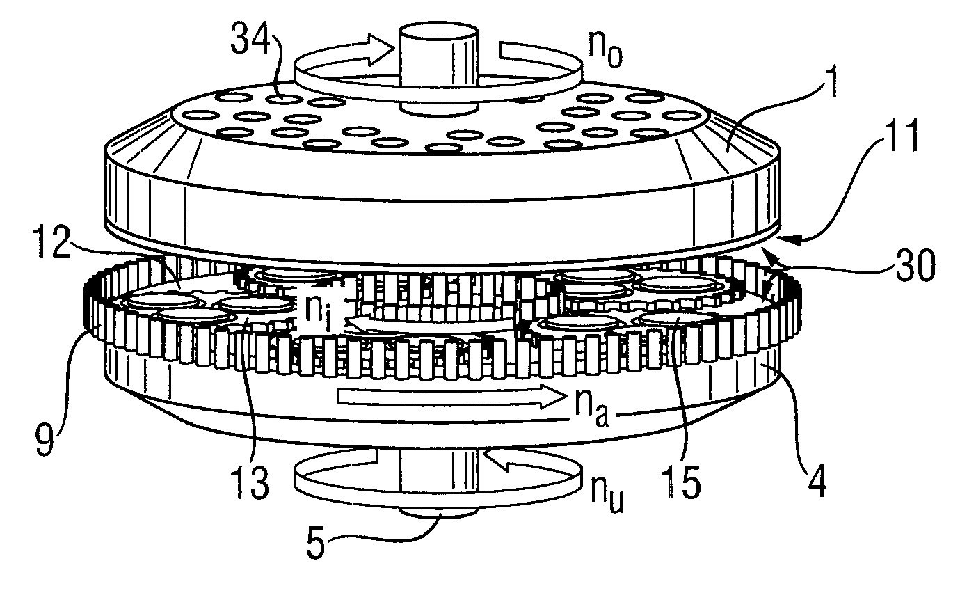
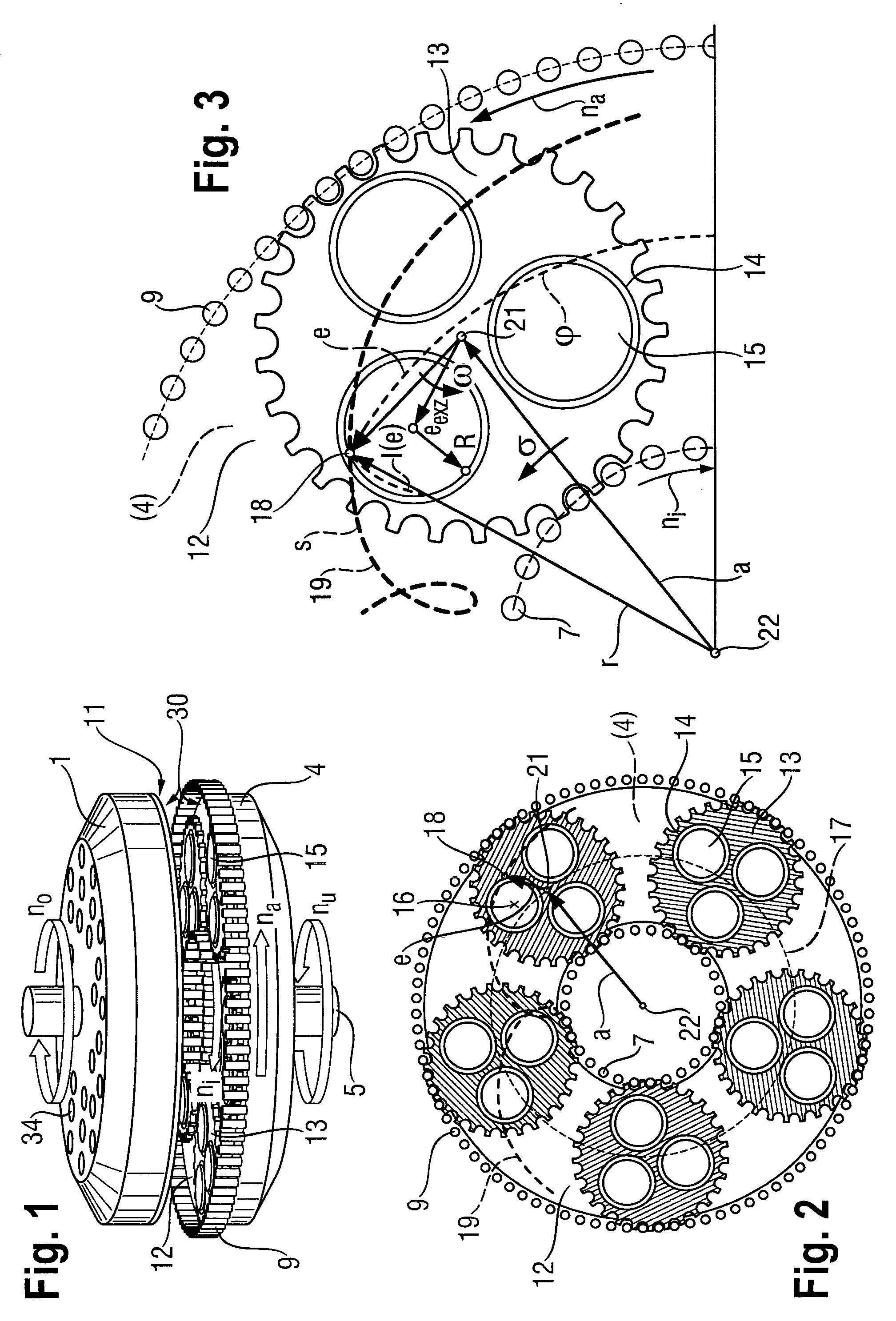
[0187]Since the working disks are composed of different materials having correspondingly different coefficients of thermal expansion, a certain unavoidable deformation always occurs given an unsuitable choice of temperature on account of the “bimetal effect”. Furthermore, such a disturbance of the plane-parallelism can be effected by time-dependent temperature input during the machining sequence itself, for example as a result of the machining work performed in the working gap 30 (which leads to heating); for a temperature gradient arises as a result from the machining zone 30 into the working disks 1 and 4, and deforms the working disks (in time-dependent fashion). The semiconductor wafers machined in this...


PUM

PropertyMeasurementUnit
grain sizeaaaaaaaaaa
thicknessaaaaaaaaaa
thicknessaaaaaaaaaa

Abstract

A method for the simultaneous double-side grinding of a plurality of semiconductor wafers, involves a process wherein each semiconductor wafer lies such that it is freely moveable in a cutout of one of a plurality of carriers caused to rotate by means of a rolling apparatus and is thereby moved on a cycloidal trajectory, wherein the semiconductor wafers are machined in material-removing fashion between two rotating working disks, wherein each working disk comprises a working layer containing bonded abrasive. The method according to the invention makes it possible, by means of specific kinematics, to produce extremely planar semiconductor wafers.

Description

BACKGROUND OF THE INVENTION[0001]1. Field of the Invention[0002]The subject matter of the present invention is directed to a method for the simultaneous double-side grinding of a plurality of semiconductor wafers, wherein each semiconductor wafer lies such that it is freely moveable in a cutout of one of a plurality of carriers caused to rotate by means of a rolling apparatus and is thereby moved on a cycloidal trajectory, wherein the semiconductor wafers are machined in material-removing fashion between two rotating working disks, wherein each working disk comprises a working layer containing bonded abrasive. The subject matter of the invention is also a semiconductor wafer having outstanding flatness which can be produced by means of the method.[0003]2. Background Art[0004]Electronics, microelectronics and microelectromechanics require as starting materials (substrates), semiconductor wafers with extreme requirements for global and local flatness, single-side-referenced local flat...

Claims


Application Information

Patent Timeline
Patent Type & Authority Applications(United States)
IPC IPC(8): B24B1/00B24B37/08
CPCB24B37/08H01L21/302H01L21/304
Inventor PIETSCH, GEORGKERSTAN, MICHAEL
Owner PETER WOLTERS GMBH
Why Eureka
Try Eureka