Method for the simultaneous double-side grinding of a plurality of semiconductor wafers
a technology of semiconductor wafers and double-side grinding, which is applied in the direction of grinding machine components, manufacturing tools, lapping machines, etc., can solve the problems of affecting the performance of the grinding machine, the disadvantage of convex thickness profile of the semiconductor wafer, and the pronounced edge roll-off of the wafer, so as to prevent the edge roll-off and the effect of small line width
- Summary
- Abstract
- Description
- Claims
- Application Information
AI Technical Summary
Benefits of technology
Problems solved by technology
Method used
Image
Examples
example 1
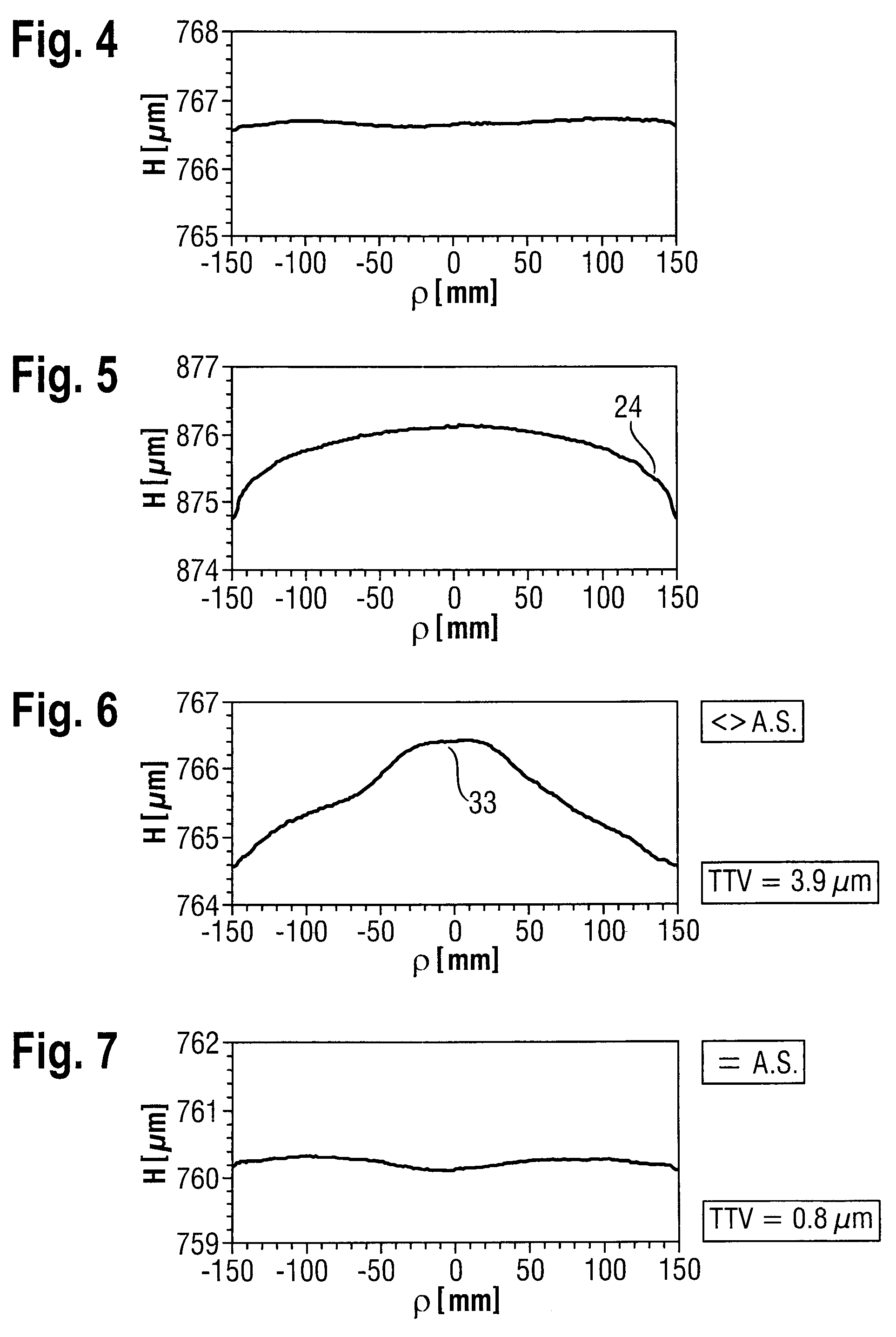
[0195]FIG. 4 shows the thickness profile of a semiconductor wafer made of monocrystalline silicon having a diameter of 300 mm which was obtained by machining by a method according to the invention having all the features of the first, second, third, fourth and fifth inventive methods. The thickness profile was determined by averaging 4 diametrically proceeding individual measurements at 0°, 45°, 90° and 135° relative to the orientation characteristic notch of the semiconductor wafer. The thickness variation over the entire semiconductor wafer (total thickness variation, TTV) is determined taking account of all the measured thickness values and amounts to 0.62 μm in this example. The thickness profiles were determined with the aid of a capacitive measuring method in which a pair of measuring probes opposite one another determines the distances with respect to the front and rear sides of the semiconductor wafer guided along between them. The edge exclusion (non-measurable edge region ...
example 2
[0196]FIG. 5 shows the thickness profile of a semiconductor wafer that is not machined according to the invention. The material removal from the semiconductor wafer was predominantly effected by free (unbonded) grain during machining (“parasitic lapping”). On account of the transport—necessary for whole-area material removal—of the free grain from the free working gap over the edge of the semiconductor wafer to the center thereof and owing to the loss of the cutting capacity of the grain on this path (wear), a depletion of grain having removal ability occurs from the edge to the center of the semiconductor wafer. Therefore, the material removal is higher at the edge than in the center of the semiconductor wafer. This results in a convex form of the semiconductor wafer with the thickness decreasing toward the edge (“edge roll-off”) 24. The TTV is 1.68 μm.
example 3
[0197]FIG. 6 shows the thickness profile of a semiconductor wafer after machining with an apparatus suitable for carrying out the claimed method in the manner according to the invention, but with working disks that are not according to the invention, namely deformed working disks.
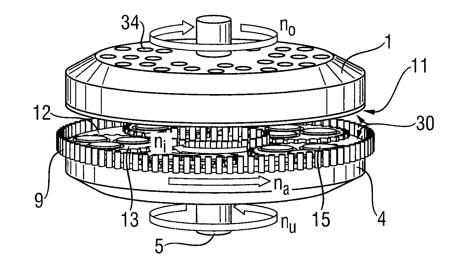
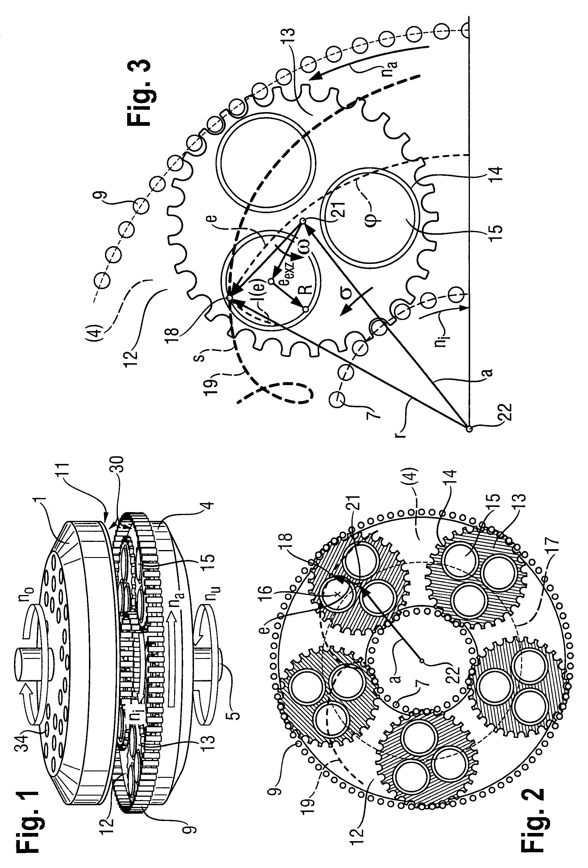
[0198]Since the working disks are composed of different materials having correspondingly different coefficients of thermal expansion, a certain unavoidable deformation always occurs given an unsuitable choice of temperature on account of the “bimetal effect”. Furthermore, such a disturbance of the plane-parallelism can be effected by time-dependent temperature input during the machining sequence itself, for example as a result of the machining work performed in the working gap 30 (which leads to heating); for a temperature gradient arises as a result from the machining zone 30 into the working disks 1 and 4, and deforms the working disks (in time-dependent fashion). The semiconductor wafers machined in this...
PUM
| Property | Measurement | Unit |
|---|---|---|
| diameter | aaaaa | aaaaa |
| RMS roughness | aaaaa | aaaaa |
| RMS roughness | aaaaa | aaaaa |
Abstract
Description
Claims
Application Information


