Wiring board, multilayer wiring board, and method for manufacturing the same

a wiring board and multi-layer technology, applied in the direction of printed circuit manufacturing, printed circuit aspects, conductive pattern formation, etc., can solve the problems of reducing size and thickness, difficulty in mounting electronic components, and reducing so as to improve the degree of flexibility in design, the effect of increasing the mounting density of components on the conductive layer surface and compactness

Inactive Publication Date: 2008-01-24
FUJIKURA LTD
View PDF11 Cites 8 Cited by
  • Summary
  • Abstract
  • Description
  • Claims
  • Application Information

AI Technical Summary

Benefits of technology

[0019] The present invention was conceived based on the above circumstances, and has as an aspect the provision of a wiring board, a multilayer wiring board using this wiring board, and a manufacturing method for these boards, which enables finer wiring patterns formed in conductive layers, while also raising the mounting density of components on the surfaces of conductive layers, by this means enabling greater thinness and compactness.
[0030] By this, sufficient pressing pressure may be applied to the conductive layer, so that the surface may be made flat, and consequently the component mounting density on the conductive layer surface may be increased. Further, since the conductive layer may be formed thinner compared with cases in which a plating method is used to form a conductive layer in the opening, fine wiring patterns may be formed.
[0031] Consequently, the degree of flexibility in design may be increased, and an electrical / electronic apparatus employing this wiring board may be made thinner, more compact, and lighter in weight.

Problems solved by technology

If a recess is generated in the conductive layer 106, it becomes difficult to mount an electronic component or the like in this portion, and the component mounting density is reduced, which is a disadvantage from the standpoint of reducing size and thickness.
Consequently, in the wiring board 100B, the conductive layer is thick, and formation of fine wiring patterns is difficult.
However, in such a multilayer wiring board, the conductive layer 109 must be formed so as to fill the opening 104, and thus an increase in the thickness for the conductive layer 109 is unavoidable.
As a result, formation of a fine pattern in the conductive layer 109 is difficult.
Further, the conductive layer 109 is thick and the overall thickness is increased, which are disadvantageous for the reduction in the size and the thickness of the electrical / electronic apparatus.

Method used


Image

  • Wiring board, multilayer wiring board, and method for manufacturing the same
  • Wiring board, multilayer wiring board, and method for manufacturing the same
  • Wiring board, multilayer wiring board, and method for manufacturing the same

Examples


first embodiment

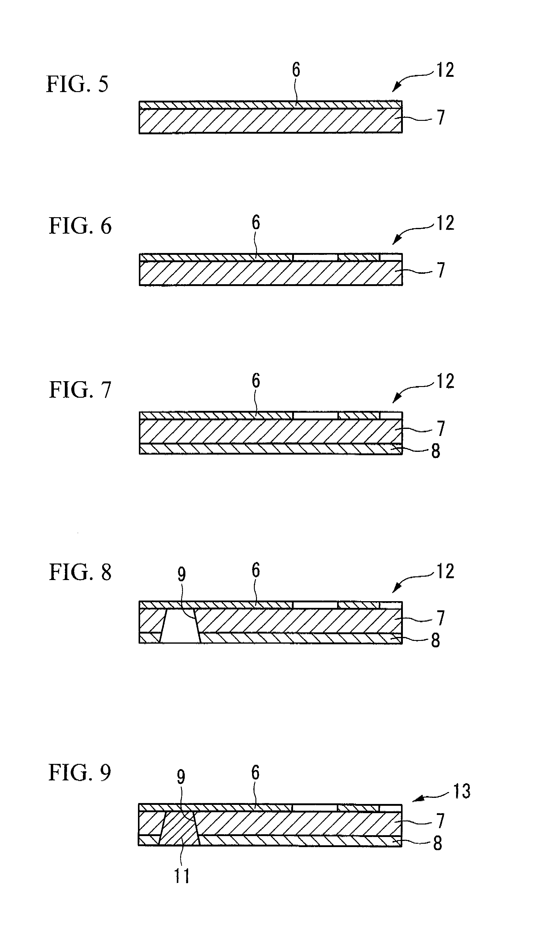
[0129] The manufacturing method of this embodiment differs from the manufacturing method of the first embodiment in that, after first stacking onto the wiring board 10 an outer-layer wiring substrate 13 on which a wiring pattern has not yet been formed, the wiring pattern is formed in the outer layer-side conductive layer 6. The following is a detailed explanation.

[0130] As shown in FIG. 14 and FIG. 15, outer-layer wiring substrates 13 in the outer layer-side conductive layers 6 of which a wiring pattern has not been formed are stacked onto both surfaces of a wiring board 10, and by performing pressing in the thickness direction, the outer-layer wiring substrates 13 and wiring board 10 are bonded together.

[0131] Next, as shown in FIG. 16, a pattern of wiring is formed in the outer layer-side conductive layers 6 of the outer-layer wiring substrates 13, to obtain the multilayer wiring board 15.

[0132] As shown in FIG. 17 and FIG. 18, additional layers may be added to the multilayer w...

second embodiment

[0134] According to the manufacturing method of the above second embodiment, since a wiring pattern is formed in the outer layer-side conductive layers 6 after stacking outer-layer wiring substrates 13 onto a wiring board 10, adverse effects of the pressing process on wiring may be prevented. Hence, the wiring of the outer layer-side conductive layers 6 may be made even finer.

[0135] Next, a third nonlimiting exemplary embodiment of a method for manufacturing a multilayer wiring board of the present invention is explained.

[0136] The manufacturing method of this embodiment differs from the manufacturing method of the first embodiment in that, after first stacking onto the wiring board 10 an outer-layer wiring substrate 13a in which an opening 9 and connecting portion 11 have not yet been formed, the opening 9 and connecting portion 11 are formed. The following is a detailed explanation.

[0137] As shown in FIG. 19, outer-layer wiring substrates 13a in which an opening 9 and connecting...

third embodiment

[0141] According to the method of manufacturing of the above third embodiment, after stacking outer-layer wiring substrates 13a to a wiring board 10, the openings 9 and connecting portions 11 are formed, so that the connecting portions may be reliably brought into contact with the conducting layers 2 and 6, and the conductivity therebetween may be improved. Hence, the reliability of electrical connections may be improved.

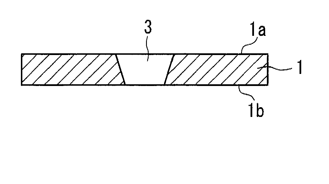
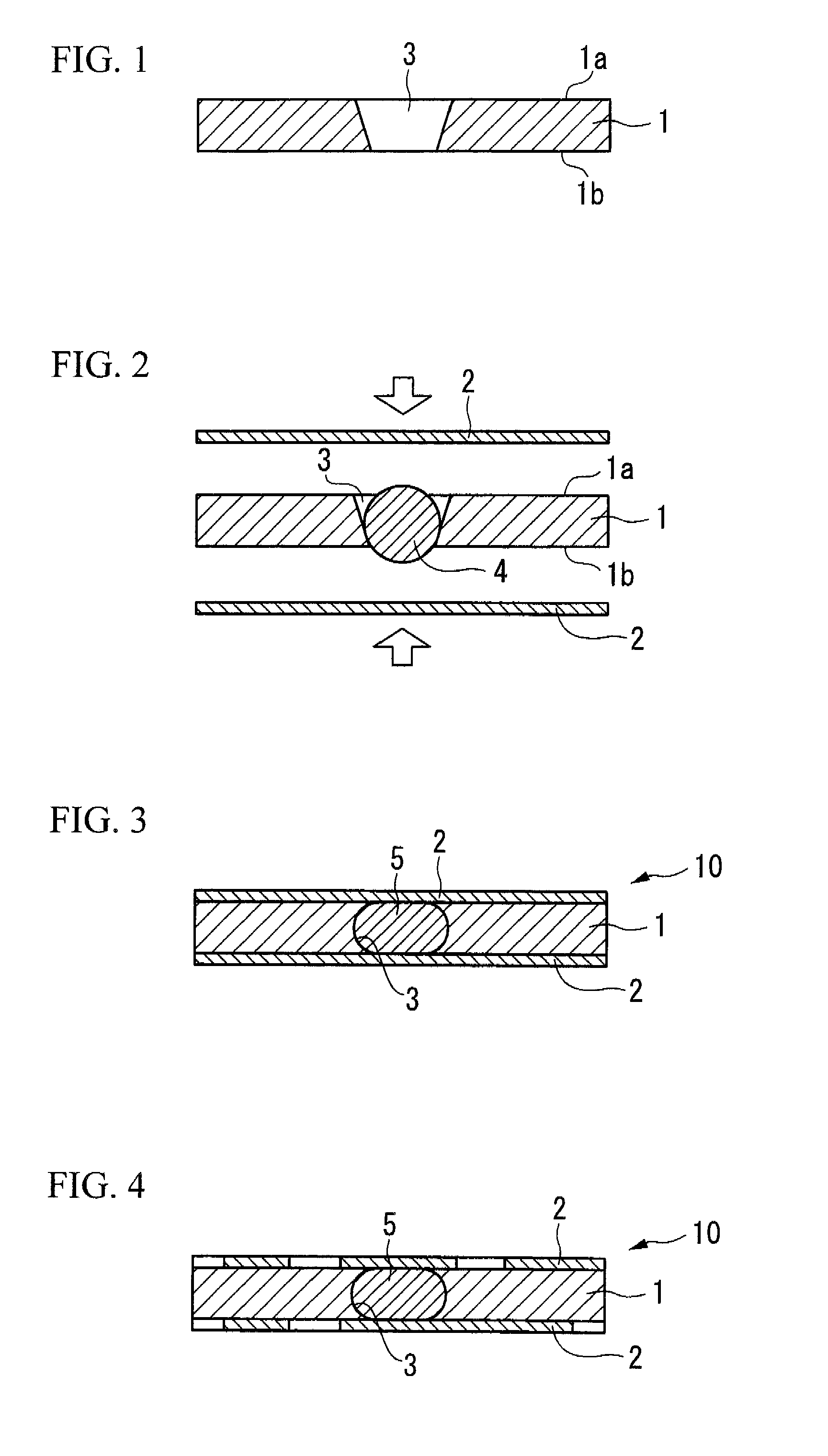
[0142] According to the manufacturing methods of the first through third embodiments, as shown in FIG. 1 through FIG. 4, when manufacturing the wiring board 10, the connecting particle 4 is placed into the penetrating hole 3, and by performing pressing in the thickness direction, the particle is deformed into the connecting member 5. However, the wiring board 10 may also be manufactured by the method described below.

[0143] As shown in FIG. 24, printing or other means are used to provide a protrusion for connection 18 on one surface (the lower surface) of an inner l...


PUM

PropertyMeasurementUnit
pressureaaaaaaaaaa
temperatureaaaaaaaaaa

Abstract

A method for manufacturing a wiring board comprising an insulating member, comprising: a penetrating hole formation process of forming a penetrating hole in the insulating member; a placement process of inserting a conductive connecting particle into the penetrating hole; a connecting particle pressing process of disposing the conductive layers on both surfaces of the insulating member, pressing the conductive layers toward the connecting particle in the penetrating hole, and deforming the connecting particle in the pressing direction to obtain the connecting member; and a patterning process of patterning the conductive layers, wherein, in the connecting particle pressing process, the pressing is performed such that the cross-sectional area in the direction along the insulating member surface of at least a portion of the connecting member is greater than the contact area of the connecting member with the conductive layers.

Description

BACKGROUND OF THE INVENTION [0001] 1. Field of the Invention [0002] The present invention relates to a wiring board in which conductive layers are formed on both surfaces of an insulating member, a multilayer wiring board in which an outer-layer wiring substrate is stacked onto at least one side of a wiring board, and a method for manufacturing these boards. [0003] Priority is claimed from Japanese Patent Application No. 2005-110653, filed Apr. 7, 2005, the content of which is incorporated herein by reference. [0004] 2. Description of the Related Art [0005]FIG. 27 shows an example of a conventional multilayer wiring board. In the multilayer wiring board shown in this figure, outer-layer wiring substrates 110 are formed on both sides of the wiring board 100A. [0006] In the wiring board 100A, conductive layers 102 are formed on both sides of the insulating member 101 having a penetrating hole (through-hole) 103. Openings are formed in the conductive layers 102 at positions correspondi...

Claims


Application Information

Patent Timeline
Patent Type & Authority Applications(United States)
IPC IPC(8): H01R43/00
CPCH05K3/386Y10T29/49117H05K3/4069H05K3/4602H05K3/4617H05K3/4647H05K3/4652H05K2201/0355H05K2201/0394H05K2201/0969H05K2201/10234H05K2203/0733H05K2203/1461Y10T29/49155H05K3/4046H05K3/46
Inventor OHARA, TOSHIHIKOUNAMI, YOSHIHARUINATANI, YUJIITO, SHOJI
Owner FUJIKURA LTD
Why Eureka
Try Eureka