Display device and semiconductor device
- Summary
- Abstract
- Description
- Claims
- Application Information
AI Technical Summary
Benefits of technology
Problems solved by technology
Method used
Image

Examples
embodiment mode 1
[0062]In this embodiment mode, a pixel structure and a layout of a display device of the present invention will be described. Note that a pixel formed of two TFTs is described here.
[0063]First, the pixel structure of the display device of the present invention is described with reference to FIG. 3. A pixel includes a TFT (driving TFT 301) connected to a pixel electrode, a capacitor 300, a switching TFT 302, a display element 303, a scanning line 305, a signal line 304, and a power supply line 306. Note that the driving TFT 301 and the switching TFT 302 each have a double-gate structure that includes two channel formation regions.
[0064]Note that the driving TFT 301 may have a single-gate structure or a multi-gate structure that includes three or more channel formation regions.
[0065]Either one of a source terminal or drain terminal of the switching TFT 302 is connected to the signal line 304.
[0066]A gate terminal of the switching TFT 302 is connected to the scanning line 305.
[0067]The...
embodiment mode 2
[0124]In this embodiment mode, the meaning of “a longitudinal direction of a wiring” will be specifically described with reference to FIGS. 5, 6, and 7.
[0125]The “longitudinal direction of the wiring” (“channel width direction”) is the above-described “direction parallel to the direction in which current flows through the wiring arranged over the channel formation region.” Note that, in the case of a wiring having a zigzag shape or a wiring having a meander shape to be described later, current does not necessarily flow in a linear direction in the wiring. In this case, the “longitudinal direction of the wiring” (“channel width direction”) is a “direction approximately parallel to the direction in which current flows through a wiring region that is arranged over the channel formation region.”
[0126]Here, the shape of the wiring need is not necessarily a straight line as shown in FIG. 5. For example, as shown in FIG. 6, the shape of the wiring may be a zigzag shape, as first wirings 50...
embodiment mode 3
[0134]In this embodiment mode, another variation of a layout of a driving transistor of the present invention will be exemplified. Note that the present invention is not limited to the layout exemplified in this embodiment mode.
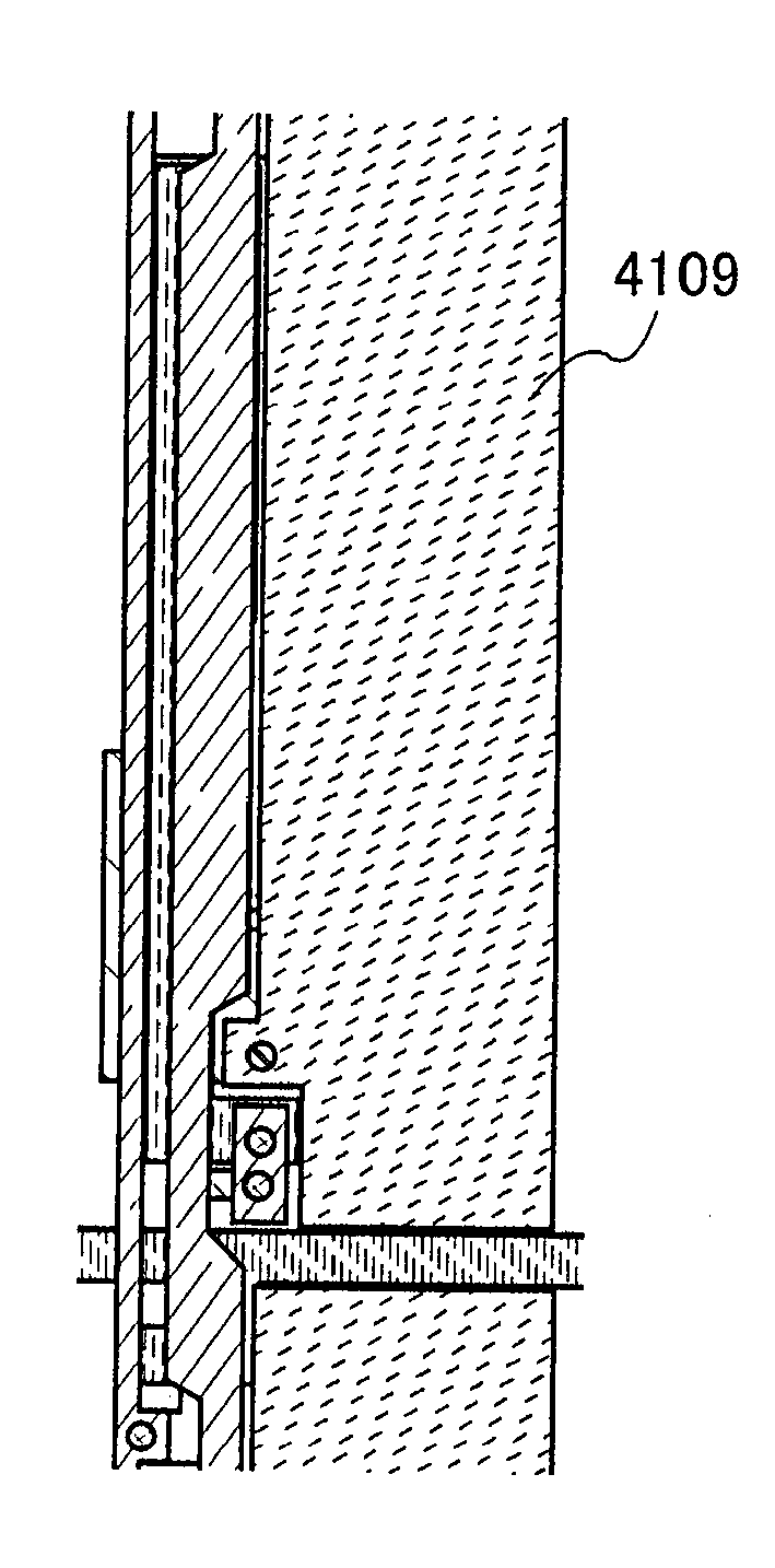
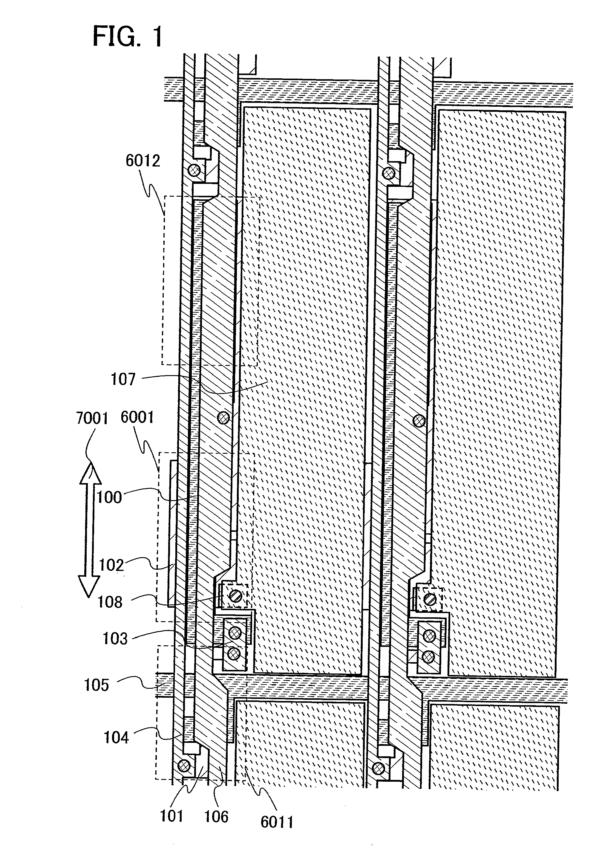
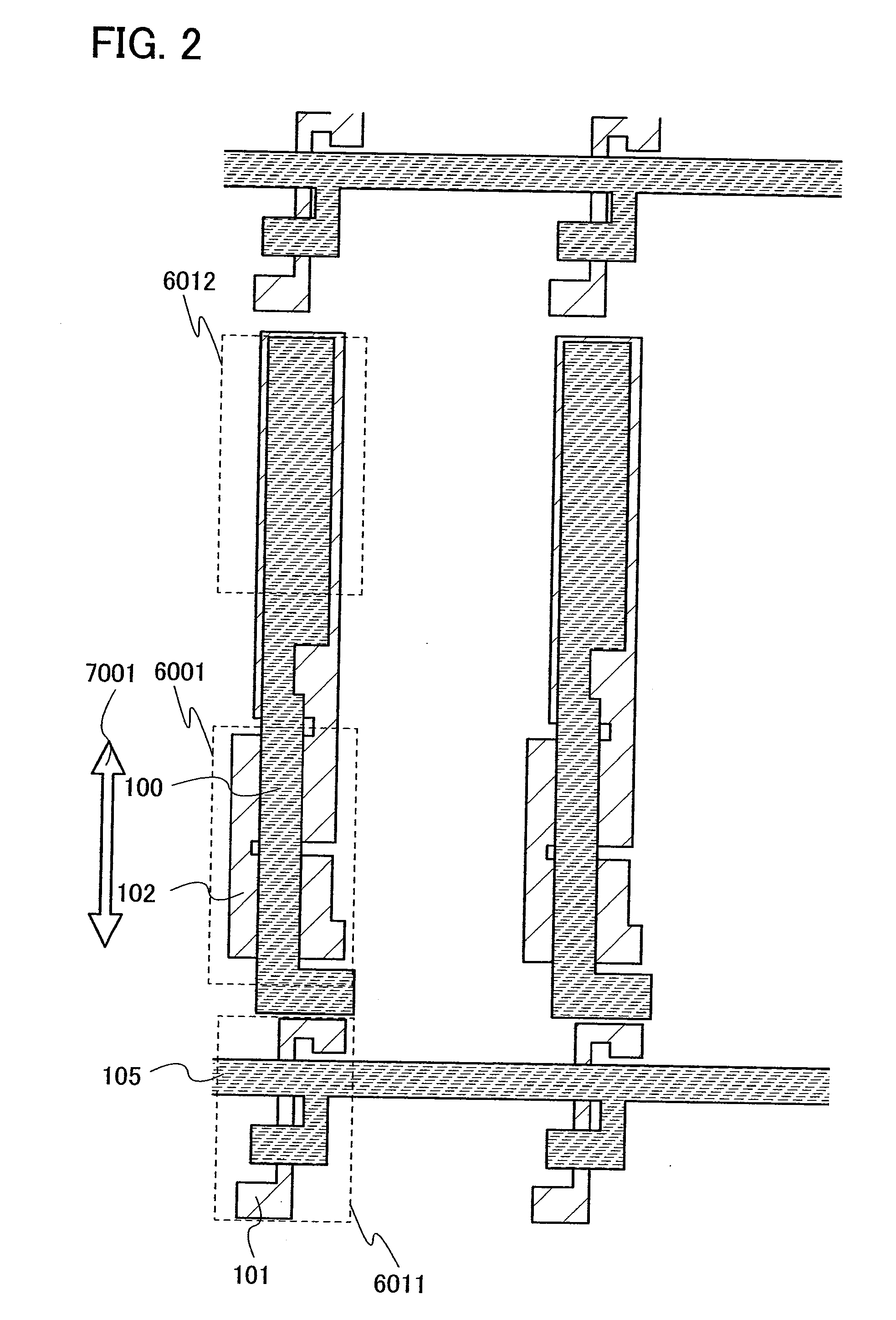
[0135]FIG. 8 shows a layout of a single-gate structure. The first semiconductor layer 101 is an island-shaped semiconductor layer of a switching TFT. A region that overlaps with the gate wiring 105 is a channel formation region. A region that is connected to the signal line 104 through a contact hole is a source terminal (or a drain terminal). A region that is connected to the connection electrode 103 is the drain terminal (or the source terminal).
[0136]Further, the second semiconductor layer 102 is the island-shaped semiconductor layer of the driving TFT 301 that drives the display element. In addition, a region that overlaps with the gate electrode 100 is a channel formation region. The gate electrode of the driving TFT 301 is connected to the connection el...
PUM
 Abstract
Description
Claims
Application Information
 - R&D
- Intellectual Property
- Life Sciences
- Materials
- Tech Scout
- Unparalleled Data Quality
- Higher Quality Content
- 60% Fewer Hallucinations
Browse by: Latest US Patents, China's latest patents, Technical Efficacy Thesaurus, Application Domain, Technology Topic, Popular Technical Reports.
© 2025 PatSnap. All rights reserved.Legal|Privacy policy|Modern Slavery Act Transparency Statement|Sitemap|About US| Contact US: help@patsnap.com