Voltage booster for semiconductor device and semiconductor memory device using same

a voltage booster and semiconductor technology, applied in the direction of dc-dc conversion, power conversion systems, digital storage, etc., can solve the problems of undesirable turning of the third pmos transistor pb>3/b>, unreliable operation of the semiconductor device, etc., and achieve the effect of reducing the voltage level

Active Publication Date: 2008-01-24
SAMSUNG ELECTRONICS CO LTD
View PDF12 Cites 32 Cited by
  • Summary
  • Abstract
  • Description
  • Claims
  • Application Information

AI Technical Summary

Benefits of technology

[0026]According to one embodiment of the invention, a voltage booster for a semiconductor device having a normal mode and a power-saving mode comprises a level shifter, an initial voltage booster, and a voltage boosting circuit. The level shifter is configured to receive a power-up signal and generate a level shifter output signal in response to the power-up signal, wherein the power-up signal increases along with an internal power supply voltage generated using an external power supply voltage and makes a logical transition when the internal power supply voltage reaches an predetermined internal power supply voltage target level. The initial voltage booster is configured to transmit the external power supply voltage through an initial boosting node to a voltage boosting terminal in response to the level shifter output signal during the normal mode, and to block transmission of the external power supply voltage to the initial boosting node to decrease a voltage level of the initial boosting node during the power-saving mode. The voltage boosting circuit is configured to perform a charge pumping operation in response to the power-up signal to generate a boosting voltage with an amplitude higher than an amplitude of the external power supply voltage during the normal mode and further configured to disable the charge pumping operation during the power-saving mode.
[0027]According to another embod

Problems solved by technology

In general, the operation of a semiconductor device is unreliable until the internal operating voltages stabilize during some period of time after

Method used


Image

  • Voltage booster for semiconductor device and semiconductor memory device using same
  • Voltage booster for semiconductor device and semiconductor memory device using same
  • Voltage booster for semiconductor device and semiconductor memory device using same

Examples


Embodiment Construction

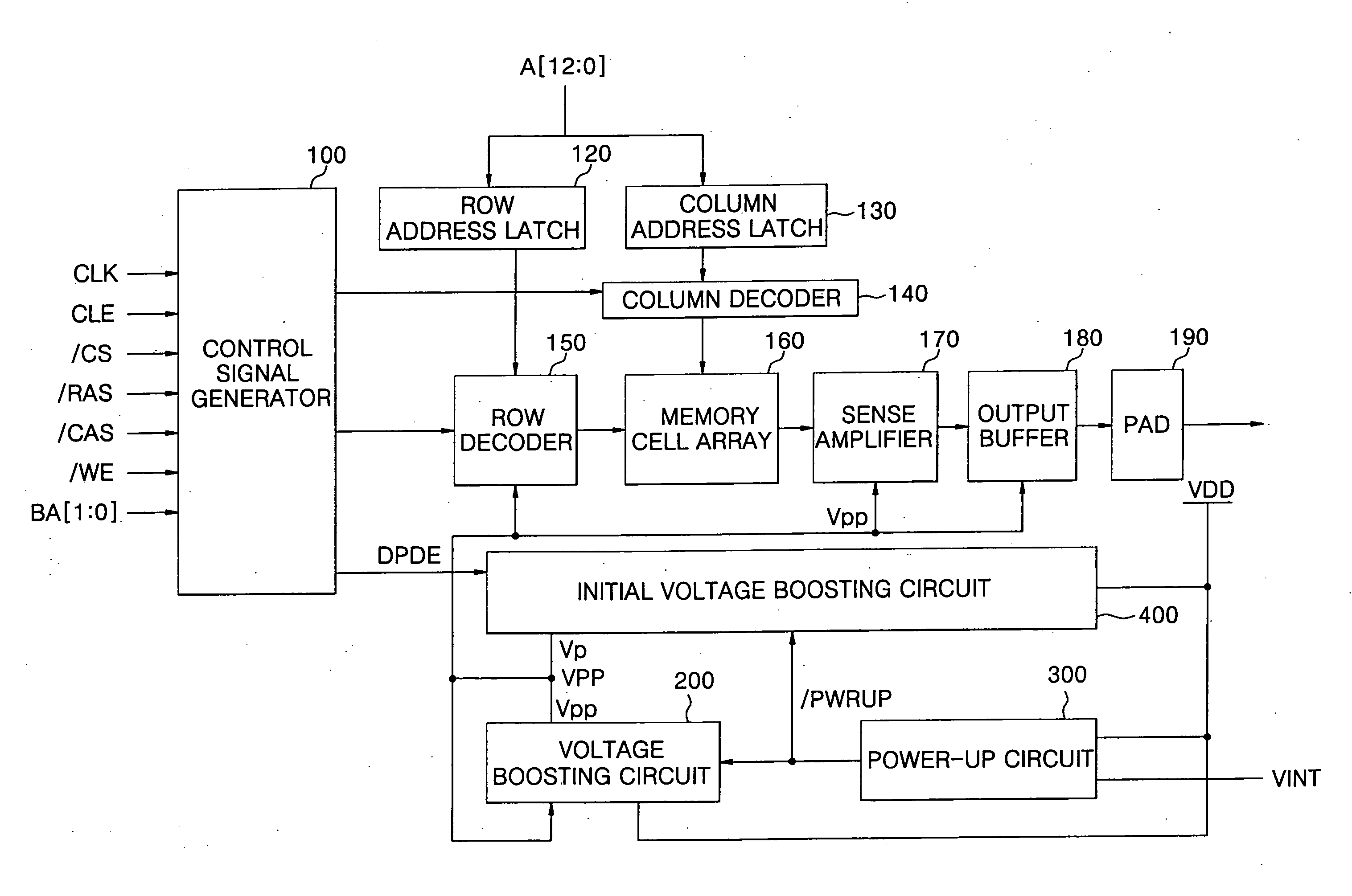
[0037]Exemplary embodiments of the invention are described below with reference to the corresponding drawings. These embodiments are presented as teaching examples and the actual scope of the invention is defined by the claims that follow. In general, various embodiments of the invention described below provide voltage boosters and semiconductor memory devices using the voltage boosters.

[0038]FIG. 3 is a block diagram of a voltage booster for a semiconductor device according to one embodiment of the invention. Referring to FIG. 3, the voltage booster comprises a voltage boosting circuit 200, a power-up circuit 300, and an initial voltage boosting circuit 400. Initial voltage boosting circuit 400 comprises a level shifter 410 and an initial voltage booster 420.

[0039]Voltage boosting circuit 200 receives power-up signal / PWRUP from power-up circuit 300, and a fed-back boosting voltage Vpp, and outputs boosting voltage Vpp. Where power-up signal / PWRUP has logic level “low, voltage boo...


PUM


Abstract

A semiconductor device has a power-saving mode and a normal mode. A voltage booster within the semiconductor device responds to the normal mode and the power-saving mode by controlling various internal operating voltages of the semiconductor device using a level shifter, an internal voltage booster, and a voltage boosting circuit. The initial voltage booster is configured to transmit an external power supply voltage through an initial boosting node to a voltage boosting terminal in response to the level shifter output signal during the normal mode, and to block transmission of the external power supply voltage to the initial boosting node to decrease a voltage level of the initial boosting node during the power-saving mode.

Description

BACKGROUND OF THE INVENTION[0001]1. Field of the Invention[0002]Embodiments of the invention relate generally to a voltage booster for a semiconductor device. More particularly, embodiments of the invention relate to a voltage booster and associated initial voltage boosting circuit adapted for use in a semiconductor device having a power-saving mode.[0003]A claim of priority is made to Korean Patent Application No. 2006-0067040 filed on Jul. 18, 2006, the disclosure of which is hereby incorporated by reference in its entirety.[0004]2. Description of Related Art[0005]Modern semiconductor devices tend to operate using relatively low internal operating voltages. The relatively low internal operating voltages are typically generated by applying a relatively high external power supply voltage to the semiconductor devices and then stepping down the relatively high external power supply voltage. Initial application of an external power supply voltage to a semiconductor device and subsequen...

Claims


Application Information

Patent Timeline
IPC IPC(8): G05F1/10G11C5/14
CPCG11C5/145G11C11/4074G11C11/4072G11C7/20
Inventor SHIN, CHANG-HO
Owner SAMSUNG ELECTRONICS CO LTD
Why Eureka
Try Eureka