Inspection method and apparatus, lithographic apparatus, lithographic processing cell and device manufacturing method

a technology of lithographic processing cell and manufacturing method, which is applied in the direction of printers, instruments, photographic processes, etc., can solve the problems of significant errors and inability to reuse the relationship derived

Active Publication Date: 2008-01-24
ASML NETHERLANDS BV
View PDF9 Cites 47 Cited by
  • Summary
  • Abstract
  • Description
  • Claims
  • Application Information

AI Technical Summary

Problems solved by technology

Thus, the calibration array must be printed and measured in each layer in which targets are to be measured in each manufacturing process, it is not possible to reuse the relationship derived from one layer in one process in a different layer or process.
A limitation of the principal component analysis technique is that unintended variations in the underlying structure, e.g. layer thickness variations, between the calibration substrate and the substrate being measured can lead to significant errors.

Method used


Image

  • Inspection method and apparatus, lithographic apparatus, lithographic processing cell and device manufacturing method
  • Inspection method and apparatus, lithographic apparatus, lithographic processing cell and device manufacturing method
  • Inspection method and apparatus, lithographic apparatus, lithographic processing cell and device manufacturing method

Examples


Embodiment Construction

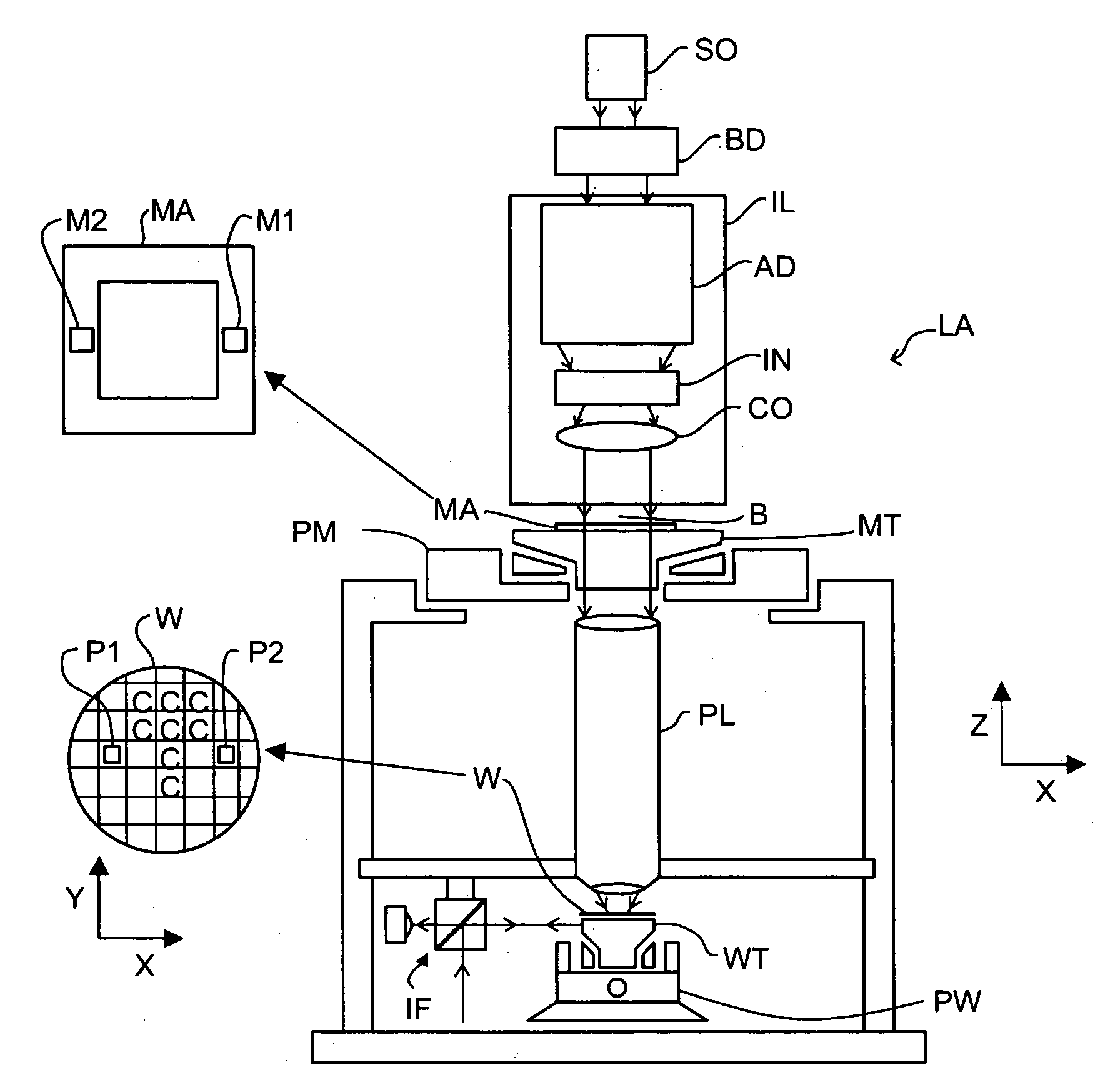
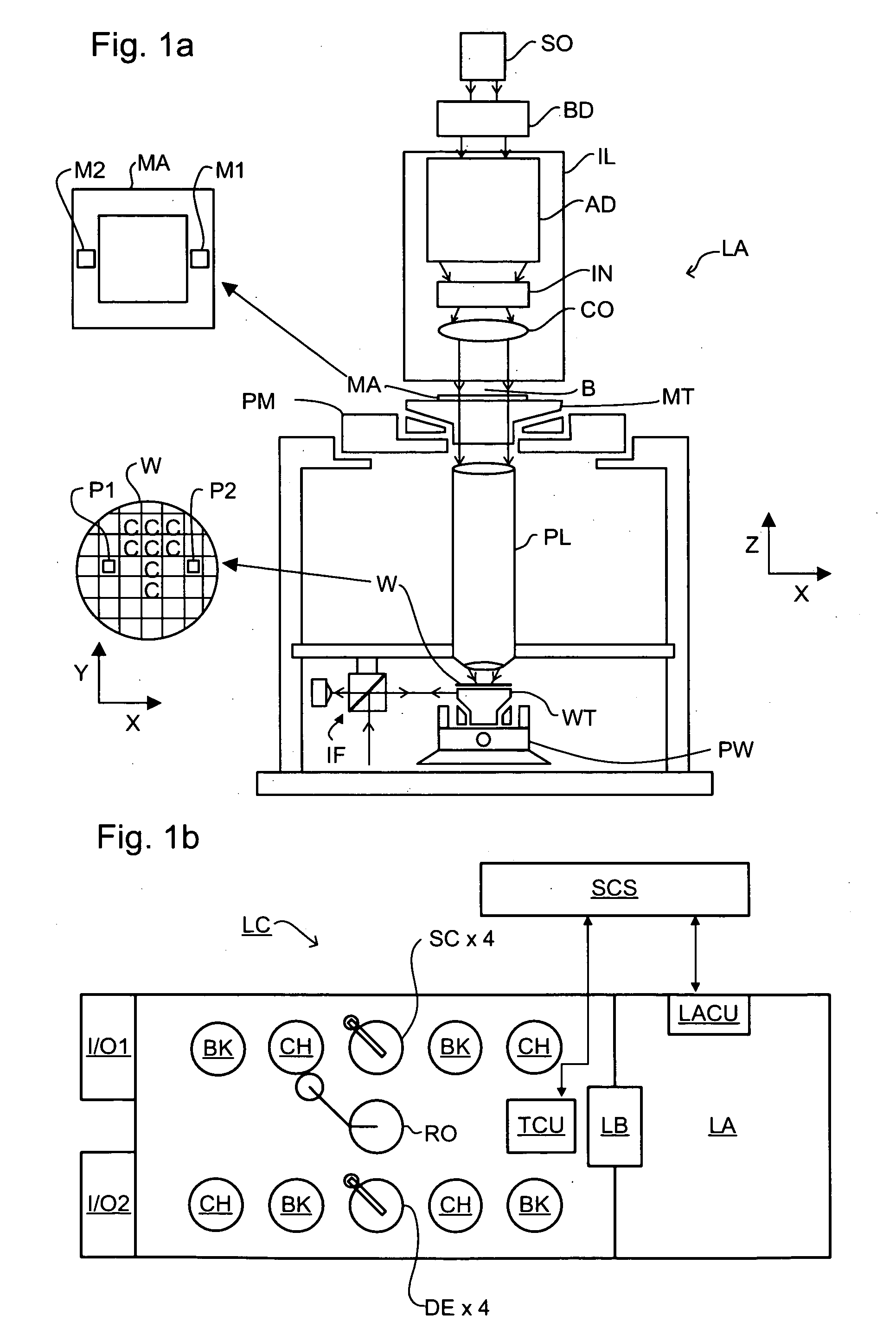
[0027]FIG. 1a schematically depicts a lithographic apparatus. The apparatus comprises an illumination system (illuminator) IL configured to condition a radiation beam B (e.g. UV radiation or EUV radiation). A support (e.g. a mask table) MT configured to support a patterning device (e.g. a mask) MA and connected to a first positioner PM configured to accurately position the patterning device in accordance with certain parameters. A substrate table (e.g. a wafer table) WT is configured to hold a substrate (e.g. a resist coated wafer) W and is connected to a second positioner PW configured to accurately position the substrate in accordance with certain parameters. A projection system (e.g. a refractive projection lens system) PL configured to project a pattern imparted to the radiation beam B by patterning device MA onto a target portion C (e.g. comprising one or more dies) of the substrate W.

[0028]The illumination system may include various types of optical components, such as refract...


PUM


Abstract

In a scatterometric method differential targets with different sensitivities to parameters of interest are printed in a calibration matrix and difference spectra obtained. principal component analysis is applied to the difference spectra to obtain a calibration function that is less sensitive to variations in the underlying structure than a calibration function obtained from spectra obtained from a single target.

Description

BACKGROUND OF THE INVENTION[0001]1. Field of the Invention[0002]The present invention relates to methods of inspection usable, for example, in the manufacture of devices by lithographic techniques and to methods of manufacturing devices using lithographic techniques.[0003]2. Description of the Related Art[0004]A lithographic apparatus is a machine that applies a desired pattern onto a substrate, usually onto a target portion of the substrate. A lithographic apparatus can be used, for example, in the manufacture of integrated circuits (ICs). In that instance, a patterning device, which is alternatively referred to as a mask or a reticle, may be used to generate a circuit pattern to be formed on an individual layer of the IC. This pattern can be transferred onto a target portion (e.g. comprising part of, one, or several dies) on a substrate (e.g. a silicon wafer). Transfer of the pattern is typically via imaging onto a layer of radiation-sensitive material (resist) provided on the sub...

Claims


Application Information

Patent Timeline
Patent Type & Authority Applications(United States)
IPC IPC(8): G03B27/52
CPCG03F7/70516G03F7/70616G03F7/70683G03F7/70641G03F7/70625G03F7/70491
Inventor DUSA, MIRCEABOEF, ARIE JEFFREY DENCRAMER, HUGO AUGUSTINUS JOSEPH
Owner ASML NETHERLANDS BV
Why Eureka
Try Eureka