Twisted Dual-Substrate Orientation (DSO) Substrates

a substrate and dual-substrate technology, applied in the field of twisted dual-substrate orientation substrates, can solve the problems of difficult patterning and inability to be readily integrated

Inactive Publication Date: 2008-01-24
TAIWAN SEMICON MFG CO LTD
View PDF7 Cites 76 Cited by
  • Summary
  • Abstract
  • Description
  • Claims
  • Application Information

AI Technical Summary

Problems solved by technology

Such an alignment occupies more area, is difficult to pattern with advanced lithogr

Method used


Image

  • Twisted Dual-Substrate Orientation (DSO) Substrates
  • Twisted Dual-Substrate Orientation (DSO) Substrates
  • Twisted Dual-Substrate Orientation (DSO) Substrates

Examples


Embodiment Construction

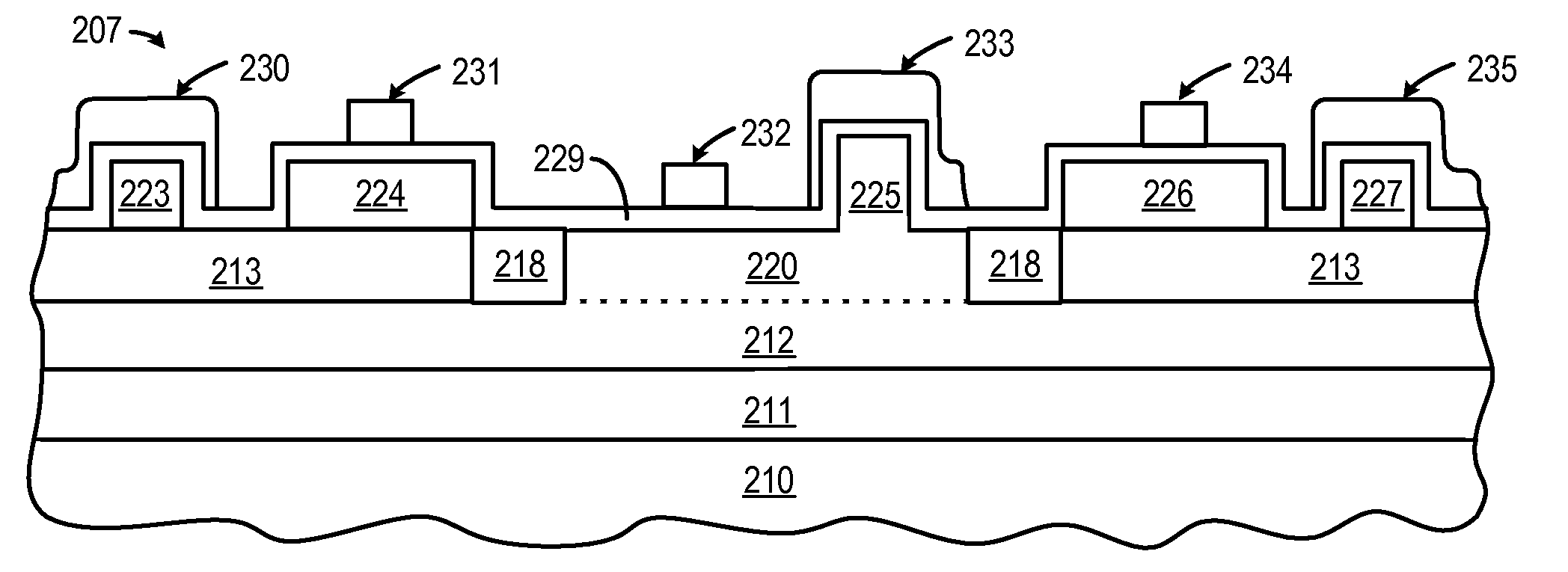
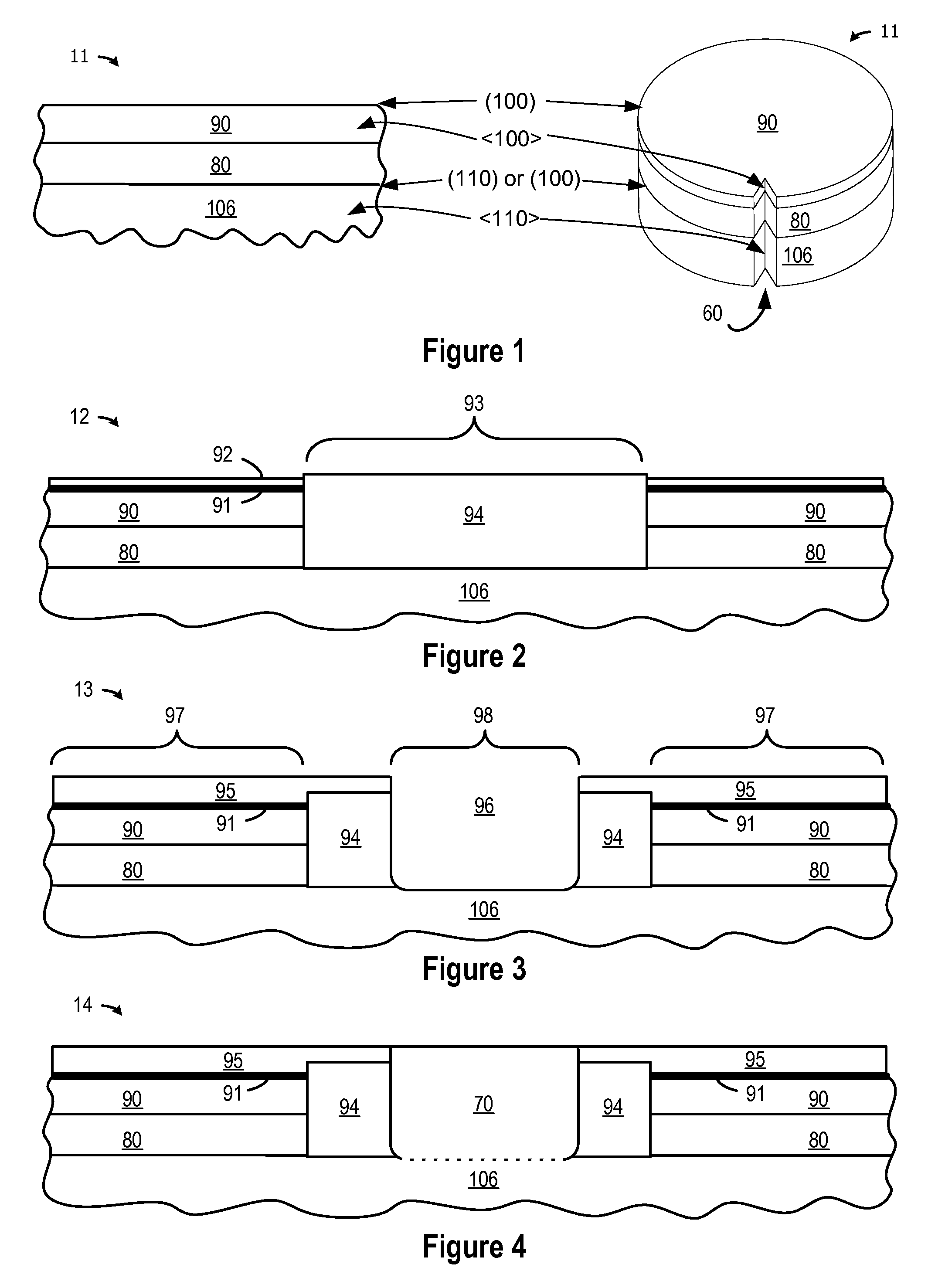
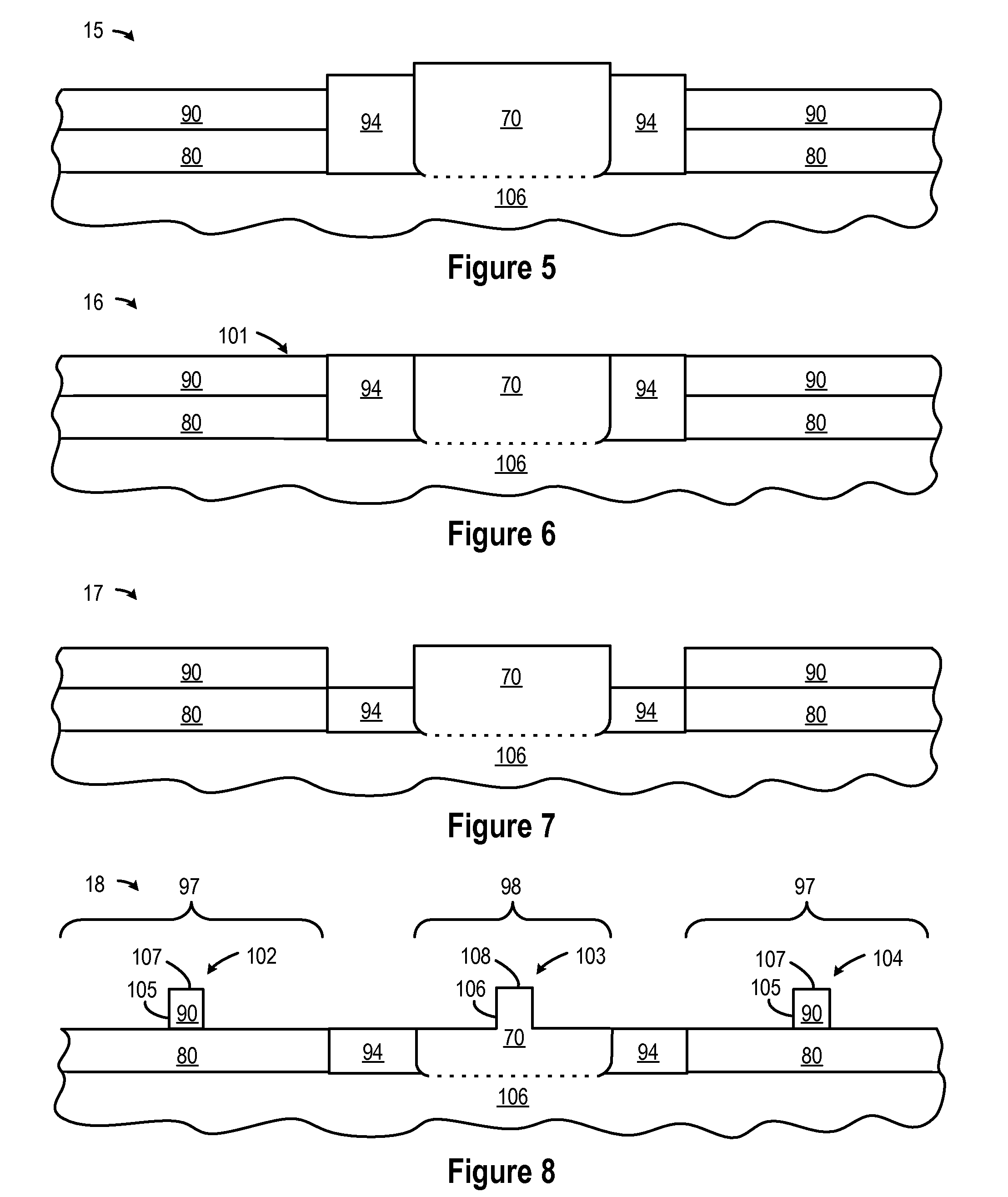
[0025]A method and apparatus are described for fabricating high performance CMOS FinFET devices with hybrid or dual substrates by selectively growing epitaxial semiconductor to partially or completely fill a trench opening formed in a shallow trench isolation region, thereby forming a first substrate (e.g., an epitaxial semiconductor layer) that is isolated by the shallow trench isolation region from a second substrate (e.g., an SOI semiconductor layer). After selectively etching part of the shallow trench isolation region down to a buried SOI insulator layer, the first substrate (epitaxial semiconductor layer) and second substrate (SOI semiconductor layer) are patterned and etched to form the channel or body portions of FinFET transistor devices over first and second substrates. By separately forming the first and second substrates with different, rotated crystal orientations prior to the pattern and etch steps, FinFETs and / or other planar devices having an improved performance can...


PUM


Abstract

A semiconductor process and apparatus provide a dual or hybrid substrate by forming a second semiconductor layer (214) that is isolated from, and crystallographically rotated with respect to, an underlying first semiconductor layer (212) by a buried insulator layer (213); forming an STI region (218) in the second semiconductor layer (214) and buried insulator layer (213); exposing the first semiconductor layer (212) in a first area (219) of a STI region (218); epitaxially growing a first epitaxial semiconductor layer (220) from the exposed first semiconductor layer (212); and selectively etching the first epitaxial semiconductor layer (220) and the second semiconductor layer (214) to form CMOS FinFET channel regions (e.g, 223) and planar channel regions (e.g., 224) from the first epitaxial semiconductor layer (220) and the second semiconductor layer (214).

Description

BACKGROUND OF THE INVENTION[0001]1. Field of the Invention[0002]The present invention is directed in general to the field of semiconductor devices. In one aspect, the present invention relates to high-performance complementary metal oxide semiconductor (CMOS) Fin field effect transistors (FinFETs) fabricated on hybrid or dual orientation substrates.[0003]2. Description of the Related Art[0004]Prior attempts to address the difference in electron and hole mobility values for NMOS and PMOS FinFET devices formed on the surface of semiconductor wafers having a single crystal orientation have aligned the channels of the NMOS FinFETs at a 45 degree angle with respect to the channels of the PMOS FinFETs. See, for example, L. Chang et al., “Extremely Scaled Silicon Nano-CMOS Devices,”Proceedings of the IEEE, Vol. 91, No. 11, pp. 1860-1873 (November 2003). Such an alignment occupies more area, is difficult to pattern with advanced lithography techniques and is not readily integrated with plan...

Claims


Application Information

Patent Timeline
IPC IPC(8): H01L21/00
CPCH01L21/76264H01L21/845H01L27/1211H01L29/045H01L27/1207H01L29/785H01L29/7851H01L27/1203H01L29/66795
Inventor WHITE, TED R.MATHEW, LEONGUYEN, BICH-YENSHI, ZHONGHAITHEAN, VOON-YEWSADAKA, MARIAM G.
Owner TAIWAN SEMICON MFG CO LTD
Why Eureka
Try Eureka