Plasma display apparatus

a technology of display apparatus and plasma, which is applied in the direction of instruments, static indicating devices, etc., can solve the problems of generating power supply noise, affecting the surrounding environment, and affecting the operation of the display apparatus, so as to reduce the load on the power supply unit, eliminate the destruction of ics and the malfunction of the circuit control, and avoid the generation of power supply noise

Inactive Publication Date: 2008-01-31
YURI SATOSHI +2
View PDF4 Cites 4 Cited by
  • Summary
  • Abstract
  • Description
  • Claims
  • Application Information

AI Technical Summary

Benefits of technology

[0037]According to at least one embodiment of the present invention, electric currents supplied from the Y-electrode drive circuit flow at different timings into at least two of the plurality of scan circuits. Accordingly, the electric currents do not flow simultaneously into these two scan circuits, thereby reducing the loa

Problems solved by technology

Consequently, a load is imposed on the power supply provided in the Y-electrode drive circuit 113, resulting in the generation of power-supply noise.
This may give rise to the problem that the destruction of ICs and the malfunction of circuit control may become more likely to

Method used


Image

  • Plasma display apparatus
  • Plasma display apparatus
  • Plasma display apparatus

Examples


Embodiment Construction

[0052]In the following, embodiments of the present invention will be described with reference to the accompanying drawings.

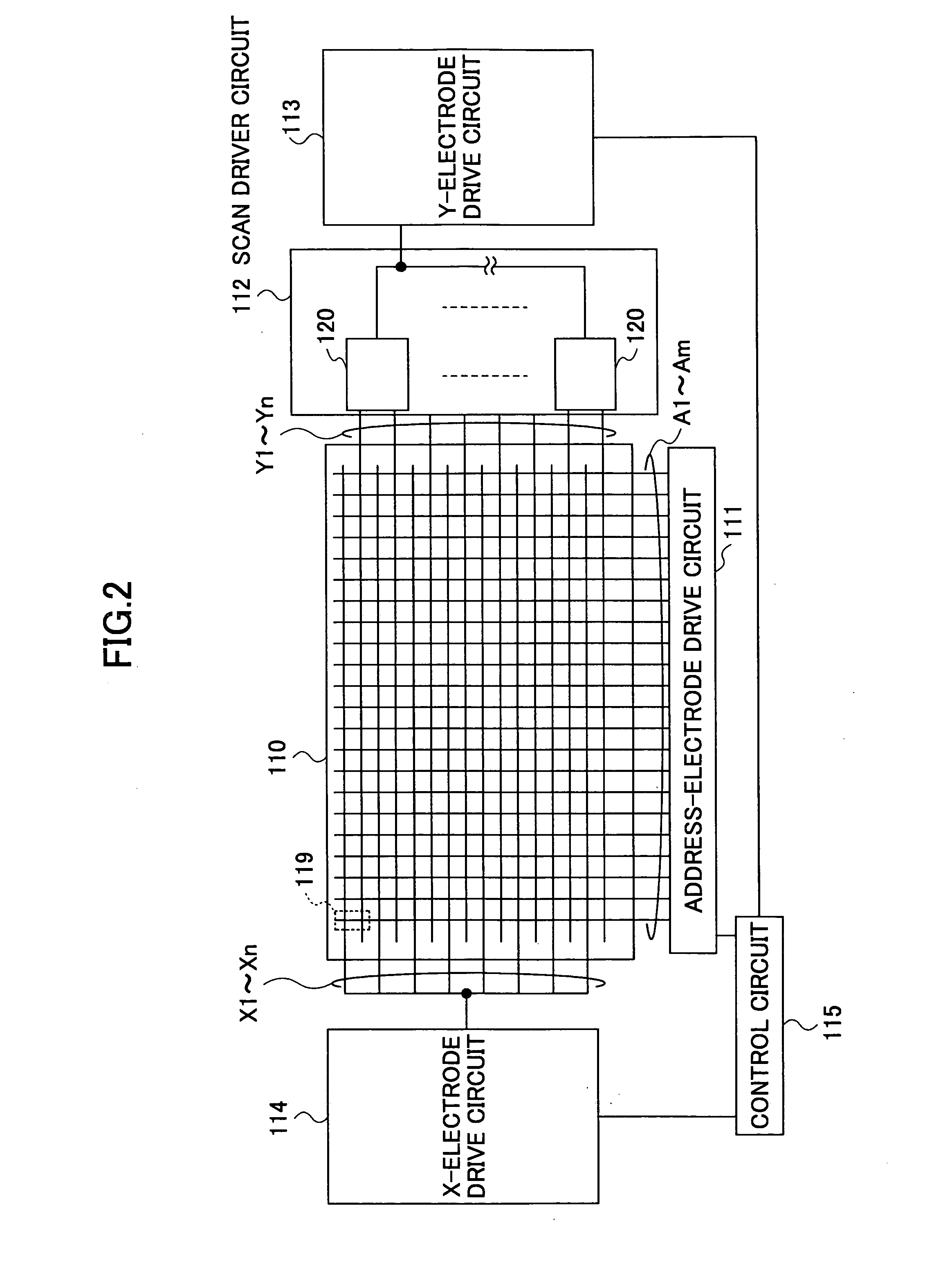
[0053]FIG. 8 is a block diagram showing a main part of a plasma display apparatus according to the present invention. In FIG. 8, the same elements as those of FIG. 2 are referred to by the same numerals, and a description thereof will be omitted.

[0054]A plasma display apparatus shown in FIG. 8 includes a plasma display panel 110, an address-electrode drive circuit 111, a scan driver circuit 112, a Y-electrode drive circuit 113, an X-electrode drive circuit 114, and a control circuit 115. The scan driver circuit 112 includes a plurality of scan driver ICs 120 and delay units 130. The delay units 130 are inserted into paths through which the output control signal OC or the power supply voltage VH is supplied from the Y-electrode drive circuit 113 to the scan driver ICs 120, and serve to delay the timing at which the output control signal OC supplied to the scan dr...


PUM


Abstract

A plasma display apparatus includes a display panel including first electrodes, second electrodes, and third electrodes, a first drive circuit configured to drive the first electrodes, a plurality of scan circuits configured to successively scan the first electrodes, a second drive circuit configured to drive the second electrodes, a third drive circuit configured to drive the third electrodes while the plurality of scan circuits successively scan the first electrodes to supply a drive power from the first drive circuit to the first electrodes, and a delay unit inserted into an interconnect connecting between at least one of the plurality of scan circuits and the first drive circuit, wherein electric currents supplied from the first drive circuit flow at different timings into at least two of the plurality of scan circuits in response to a propagation delay on the interconnect caused by the delay unit.

Description

BACKGROUND OF THE INVENTION[0001]1. Field of the Invention[0002]The present invention generally relates to plasma display apparatuses, and particularly relates to a scan driver and peripheral circuitry thereof in a plasma display apparatus.[0003]2. Description of the Related Art[0004]Flat display apparatuses using flat display panels have been put to practical use in wide areas of application from small displays to large displays, and are replacing the conventional cathode-ray tubes. A plasma display panel has two glass substrates which have electrodes formed thereon and define a space therebetween that is filled with discharge gas, and generates electric discharge by applying voltages between the electrodes so as to induce light emission from fluorescent substance provided on the substrates in response to the ultraviolet light generated by the electric discharge, thereby displaying an image. Plasma display panels are widely used as large-screen display apparatuses due to the facts ...

Claims


Application Information

Patent Timeline
IPC IPC(8): G09G3/28G09G3/288G09G3/20G09G3/291G09G3/296G09G3/298
CPCG09G3/294G09G2330/06G09G2330/025G09G3/296
Inventor YURI, SATOSHIOHNUKI, HIDENORIMACHIDA, AKIHIRO
Owner YURI SATOSHI
Why Eureka
Try Eureka