Active Matrix Substrate, Display Apparatus, and Pixel Deffect Correction Method

a technology of active matrix substrate and display apparatus, which is applied in the direction of instruments, semiconductor devices, optics, etc., can solve the problems of low aperture ratio, fatal defect in the disconnection of the electrode from the signal line, and high so as to achieve superior display quality and yield, and suppress pixel defects insufficient degree, the effect of reducing the probability of electrode disconnection

Inactive Publication Date: 2008-01-31
SHARP KK
View PDF18 Cites 22 Cited by
  • Summary
  • Abstract
  • Description
  • Claims
  • Application Information

AI Technical Summary

Benefits of technology

[0087] Further, with the manufacturing method for an ac active matrix substrate of the present invention adopting the foregoing pixel defect correction method, it becomes possible to produce an active matrix substrate capable of sufficiently suppressing the pixel defect.
[0088] Further, with the manufacturing m

Problems solved by technology

However, in the structure of liquid crystal display apparatus described in Document 5 in which the TFTs (active elements) are aligned in parallel and the electrodes connected to the signal line is required to be cut off, there are problems of low aperture ratio because of the complexity of the elect

Method used


Image

  • Active Matrix Substrate, Display Apparatus, and Pixel Deffect Correction Method
  • Active Matrix Substrate, Display Apparatus, and Pixel Deffect Correction Method
  • Active Matrix Substrate, Display Apparatus, and Pixel Deffect Correction Method

Examples


first embodiment

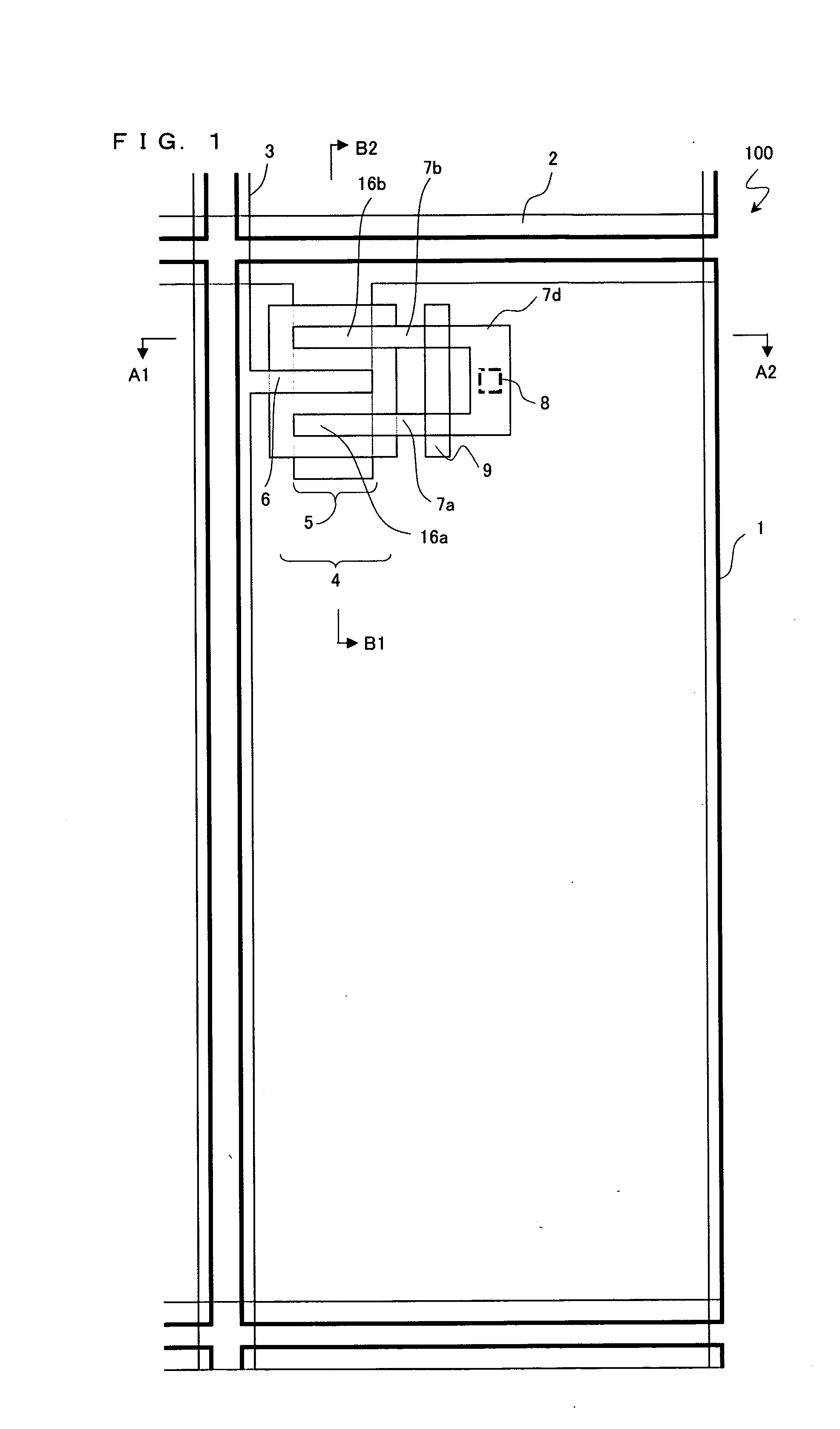
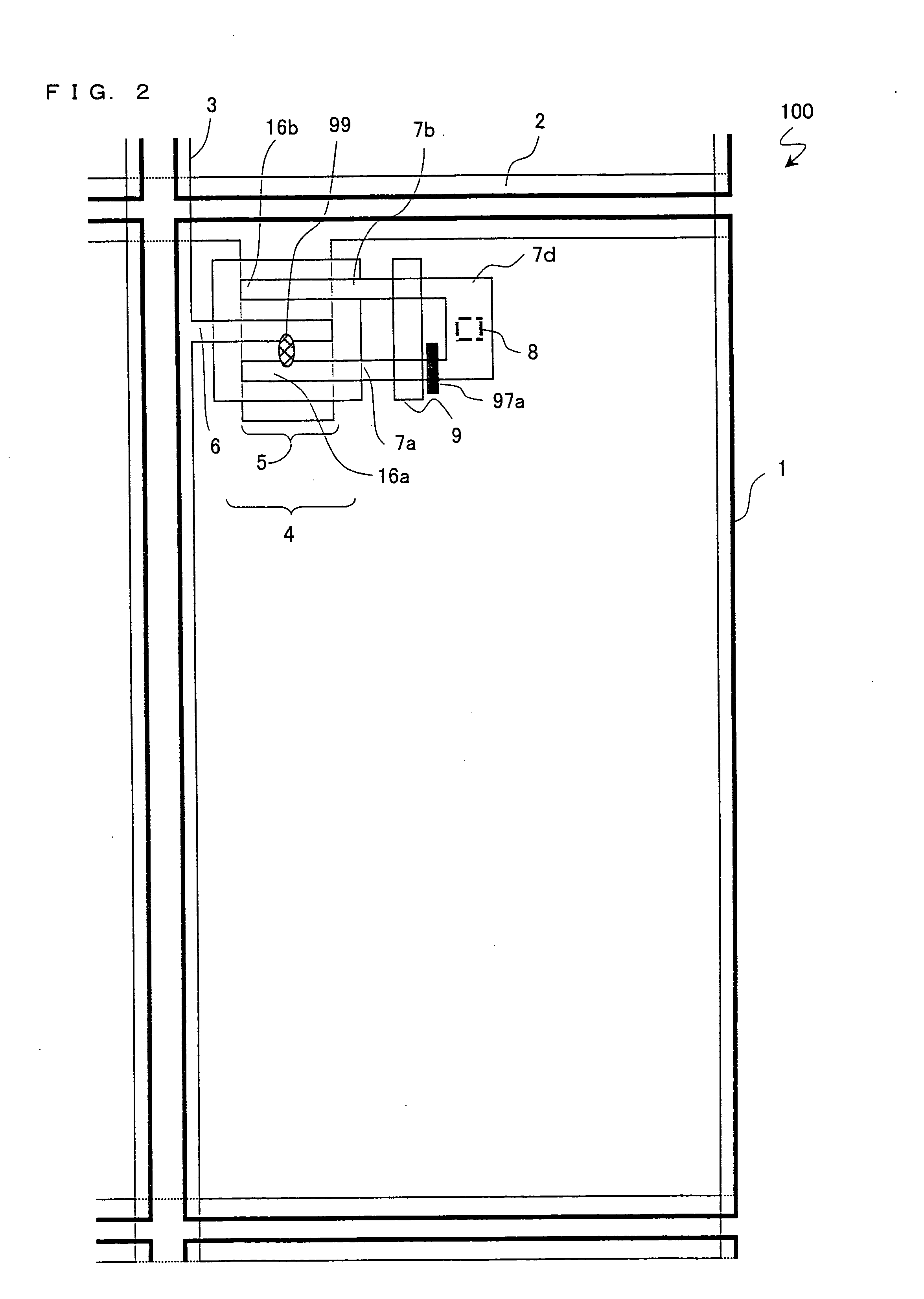
[0187] One embodiment (First Embodiment) of the present invention is first described below with reference to FIGS. 1 through 7. FIGS. 1 through 3 are schematic plan views each showing a structure of a pixel in an active matrix substrate 100 according to First Embodiment. FIG. 1 shows a structure of a pixel in which pixel defect correction is not carried out, and FIGS. 2 and 3 show a structure of a pixel in which pixel defect has been corrected. FIG. 4 is a cross-sectional view, taken along the line A1-A2 of FIG. 1. FIG. 5 is a cross-sectional view, taken along the line B1-B2 of FIG. 1. FIG. 6 is a structure view of a display apparatus including an active matrix substrate according to the present embodiment. FIG. 7 shows a structure of a television image receiver including the display apparatus of FIG. 6.

[0188] As shown in FIGS. 1 through 3, a plurality of pixel electrodes 1 are arranged on an active matrix substrate 100 in matrix. In the vicinity of the pixel electrodes 1, the scan...

second embodiment

[0213] The following describes another embodiment (Second Embodiment) of the present invention with reference to FIGS. 8 through 10. FIGS. 8 through 10 are schematic plan views showing a structure of a pixel in an active matrix substrate 100 according to Second Embodiment. FIG. 8 shows a structure of a pixel in which a pixel defect is not corrected. FIGS. 9 and 10 show a structure of a pixel having been subjected to pixel defect correction.

[0214] As shown in FIGS. 8 through 10, the active matrix substrate 100 includes a plurality of pixel electrodes 1 arranged in matrix, in the vicinity of the pixel electrodes 1, the scanning signal lines 2 for supplying scanning signals and the data signal lines 3 for supplying data signals are provided. The scanning signal lines 2 and the data signal lines 3 intersect with each other. Each of the intersections of the scanning signal lines 2 and the data signal lines 3, a TFT 4 is provided so as to serve as an active element (active element).

[021...

third embodiment

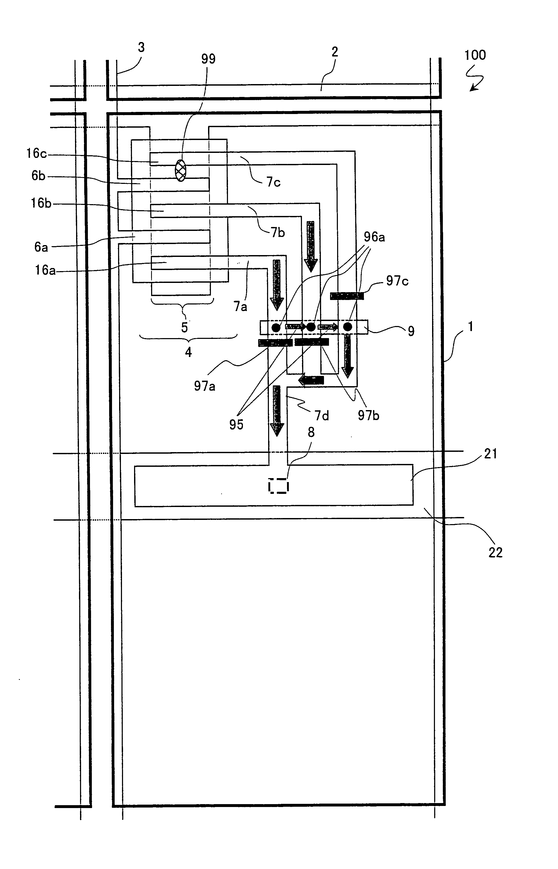
[0228] The following describes another embodiment (Third Embodiment) of the present invention with reference to FIGS. 11 through 14. FIGS. 11 through 14 are schematic plan views showing a structure of a pixel in an active matrix substrate 100 according to Third Embodiment. FIG. 11 shows a structure of a pixel in which a pixel defect is not corrected. FIGS. 12, 13 and 14 show a structure of a pixel having been subjected to pixel defect correction. In a structure shown in FIGS. 11 through 14, a single TFT includes two source electrodes 6a and 6b, and three drain electrodes 16a, 16b, and 16c. The source electrode 6a corresponds to the two drain electrodes 16a and 16b, and the source electrode 6b corresponds to two drain electrodes 16b and 16c.

[0229] As shown in FIGS. 11 through 14, the active matrix substrate 100 includes a plurality of pixel electrodes 1 arranged in matrix, in the vicinity of the pixel electrodes 1, the scanning signal lines 2 for supplying scanning signals and the d...


PUM


Abstract

An active matrix substrate is constituted of a TFT (4) in which a plurality of drain electrodes (16a and 16b) are provided for a single source electrode (6), and at least one of the drain electrodes is electrically connected to the pixel electrode (1) via the drain outgoing wire. The drain outgoing wire includes a first conductive pattern section having (i) a drain outgoing wire common section (7d) and drain outgoing branch sections (7a and 7b) each of which extends from said drain outgoing common section into each of said drain electrodes, and (ii) a correction connection electrode 9 which is partially overlapped with said branch sections of said first conductive pattern section via an insulating layer. The correction connection electrode 9 is electrically connectable to a plurality of said branch sections by being conducted to said branch sections through said insulating layer. This structure allows pixel defect correction within the pixel.

Description

TECHNICAL FIELD [0001] The present invention relates to an active matrix substrate for various display apparatuses, such as a liquid crystal display apparatus, EL (Electro Luminescence) display apparatus etc. More specifically, the present invention relates to an active matrix substrate suitable for a liquid crystal display apparatus with a large liquid crystal display screen, such as a large-size liquid crystal television. BACKGROUND ART [0002] An active matrix substrate is widely used for various active matrix display apparatuses such as a liquid crystal display apparatus, an EL (Electro Luminescence) display apparatus etc. In an active matrix substrate used for a conventional active matrix liquid crystal display apparatus, a switching element such as a TFT (Thin Film Transistor) is provided in each intersection of a plurality of scanning signal lines and a plurality of data signal lines which are intersect with each other on a base substrate. With the switching function of this s...

Claims


Application Information

Patent Timeline
IPC IPC(8): G02F1/133G02F1/1343
CPCG02F1/136259H01L27/124H01L29/41733H01L27/12G02F1/136G02F1/1368
Inventor HIRAKATA, YOSHIOTAKEUCHI, MASANORITSUBATA, TOSHIHIDE
Owner SHARP KK
Why Eureka
Try Eureka