

Photoelectric conversion apparatus and image pickup system using photoelectric conversion apparatus
a photoelectric conversion and conversion apparatus technology, applied in the field of photoelectric conversion apparatus and image pickup system using photoelectric conversion apparatus, can solve the problems of parasitic capacitance formation, asymmetric layout of photoelectric conversion elements,
- Summary
- Abstract
- Description
- Claims
- Application Information
AI Technical Summary
Problems solved by technology
Method used
Image

Examples
first exemplary embodiment
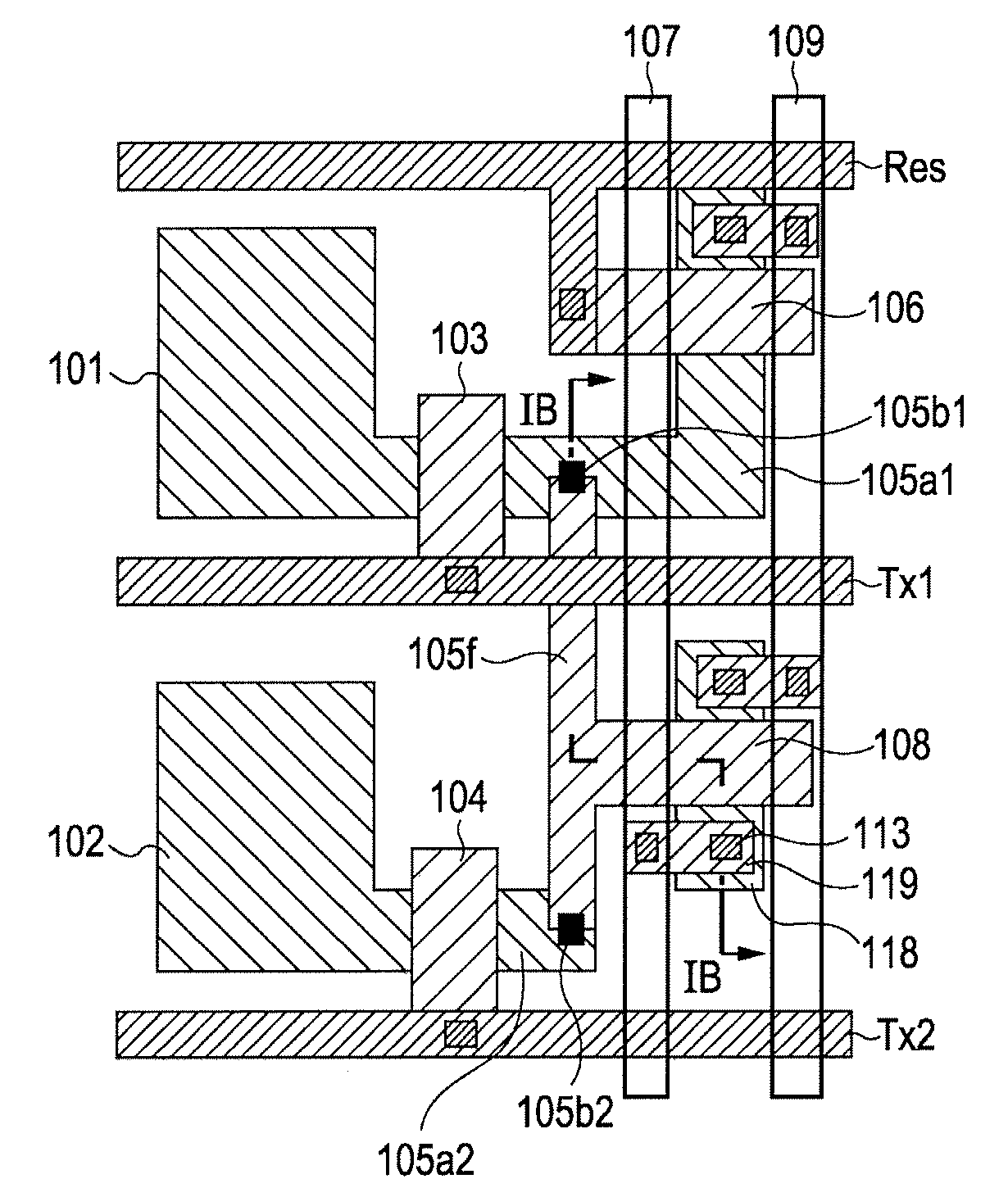
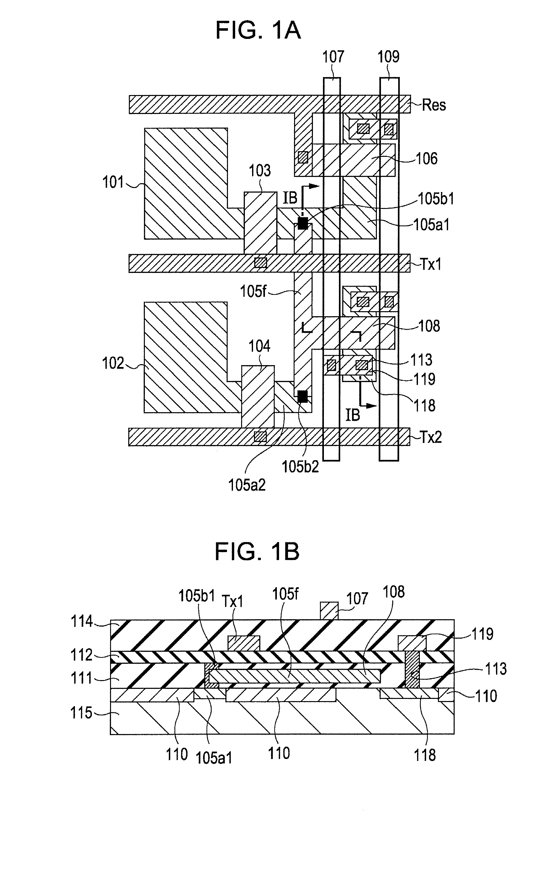
[0028]FIGS. 1A, 1B, 2A, and 2B are illustrations of a first exemplary embodiment. FIG. 3A is a circuit diagram of a photoelectric conversion apparatus according to the first exemplary embodiment. FIG. 3B shows exemplary drive pulses of the photoelectric conversion apparatus. FIG. 1A is the layout of a part of a circuit shown in FIG. 3A, the part being surrounded by a dotted line. FIG. 1B is a cross sectional view taken along line IB-IB in FIG. 1A.
[0029]The structure of the photoelectric conversion apparatus will first be described with reference to FIG. 3A. Photoelectric conversion elements 301 and 302 are connected to an FD 305 via transfer MOS transistors 303 and 304, respectively. The potential of the FD 305 is reset to a desired potential using a power supply line 309 connected to the FD 305 via a reset MOS transistor 306. Moreover, the potential of the FD 305 is input to the gate electrode of an amplifier MOS transistor 308. Signals based on the potential of the FD 305 are outp...
second exemplary embodiment
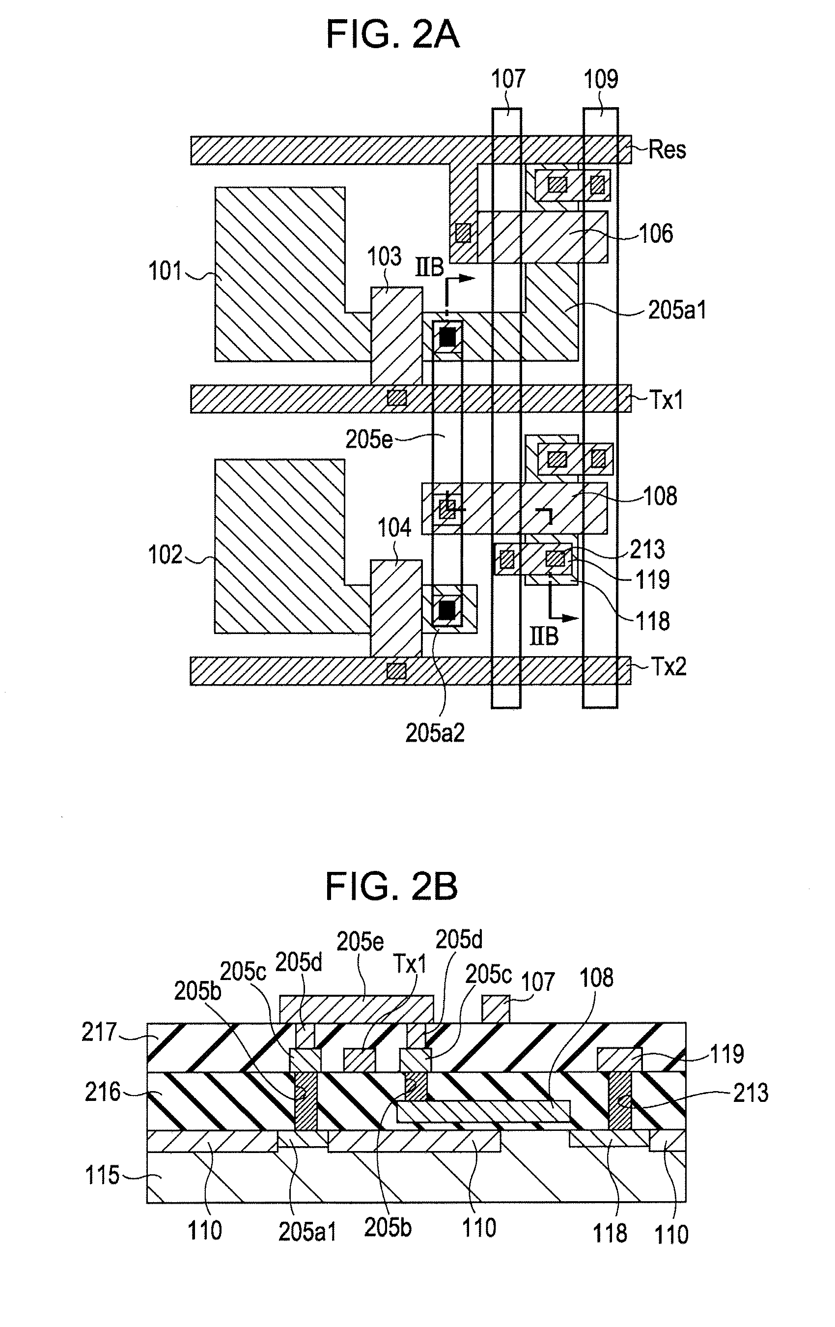
[0044]FIG. 4 shows a structure according to a second exemplary embodiment. In the second exemplary embodiment, a method for connecting the active regions of FDs and wiring lines other than the method according to the first exemplary embodiment is shown. FIG. 4 is a cross sectional view corresponding to FIG. 1A of the first exemplary embodiment. In FIG. 4, the same reference characters as in FIG. 1A are assigned to corresponding components, and the detailed description of these components is omitted here. In the second exemplary embodiment, the active region of the FD 105a1 is connected to a wiring line 405f with a contact 405b1. The polysilicon of the wiring line 405f is brought into direct contact with the FD 105a1 at the contact 405b1. When a contact having such a structure is adopted, capacitive coupling between the contact and surrounding wiring lines can be suppressed. Moreover, the insulating film 112 shown in FIG. 1B is not provided, and only insulating films 416 and 417 are ...
third exemplary embodiment
[0047]FIG. 5 shows the layout of a structure according to a third exemplary embodiment. The third exemplary embodiment is characterized in that the individual FDs of four photoelectric conversion elements are connected. That is to say, each of the FDs is separately provided for corresponding one of the photoelectric conversion elements, and the FDs are connected to a common amplifier MOS transistor. When four photoelectric conversion elements share an FD, an advantage is achieved in that the photoelectric conversion elements can be designed so that the photoelectric conversion elements are relatively large. However, in this case, FD capacitance is increased. On the other hand, in the structure according to the third exemplary embodiment, the photoelectric conversion elements can be designed so that the photoelectric conversion elements are relatively large, and FD capacitance can be reduced.
[0048]The details of the structure shown in FIG. 5 will now be described. Reference character...
PUM
 Abstract
Description
Claims
Application Information