

Distributed amplifier having a variable terminal resistance
a technology of terminal resistance and distributed amplifier, which is applied in the direction of amplifiers with semiconductor devices only, amplifiers with coupling networks, amplifiers with semiconductor devices, etc., can solve the problems of adversely affecting the gain flatness provided by the distributed amplifier, and achieve the effect of improving the gain flatness
- Summary
- Abstract
- Description
- Claims
- Application Information
AI Technical Summary
Benefits of technology
Problems solved by technology
Method used
Image

Examples
first embodiment
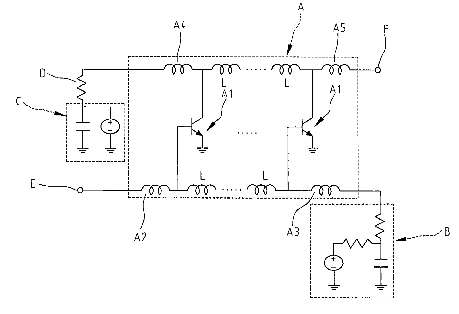
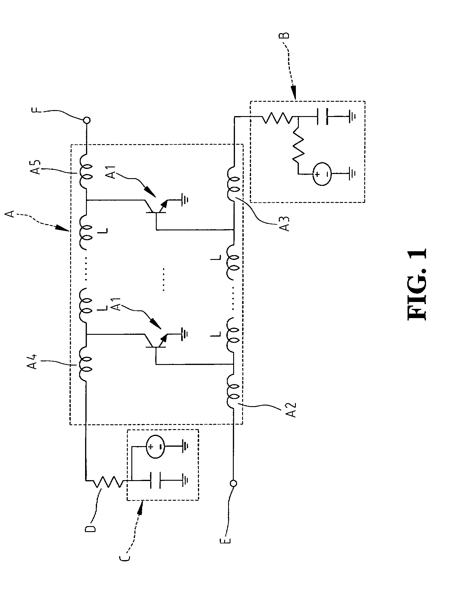
[0020]Referring to FIG. 2, a circuit diagram of a distributed amplifier having a variable terminal resistance according to the present invention is shown therein. The distributed amplifier 100 comprises a signal amplification unit 1, a first biasing circuit 2, a second biasing circuit 3, a variable terminal resistance 4, a RF signal input terminal 5 and a RF signal output terminal 6. The signal amplification unit 1 is used to amplify an input signal fed into the RF signal input terminal 5. The first biasing circuit 2 is used to provide a direct current (DC) bias signal. The second biasing circuit 3 is used to provide a DC bias signal. The variable terminal resistance 4 is disposed for providing an adjustable resistance so that a resistance matching may be achieved with respect to an output resistance of the signal amplification unit 1. The RF signal input terminal 5 is provided for input of a RF input signal. The RF signal output terminal 6 is provided for output of a RF output sign...
second embodiment
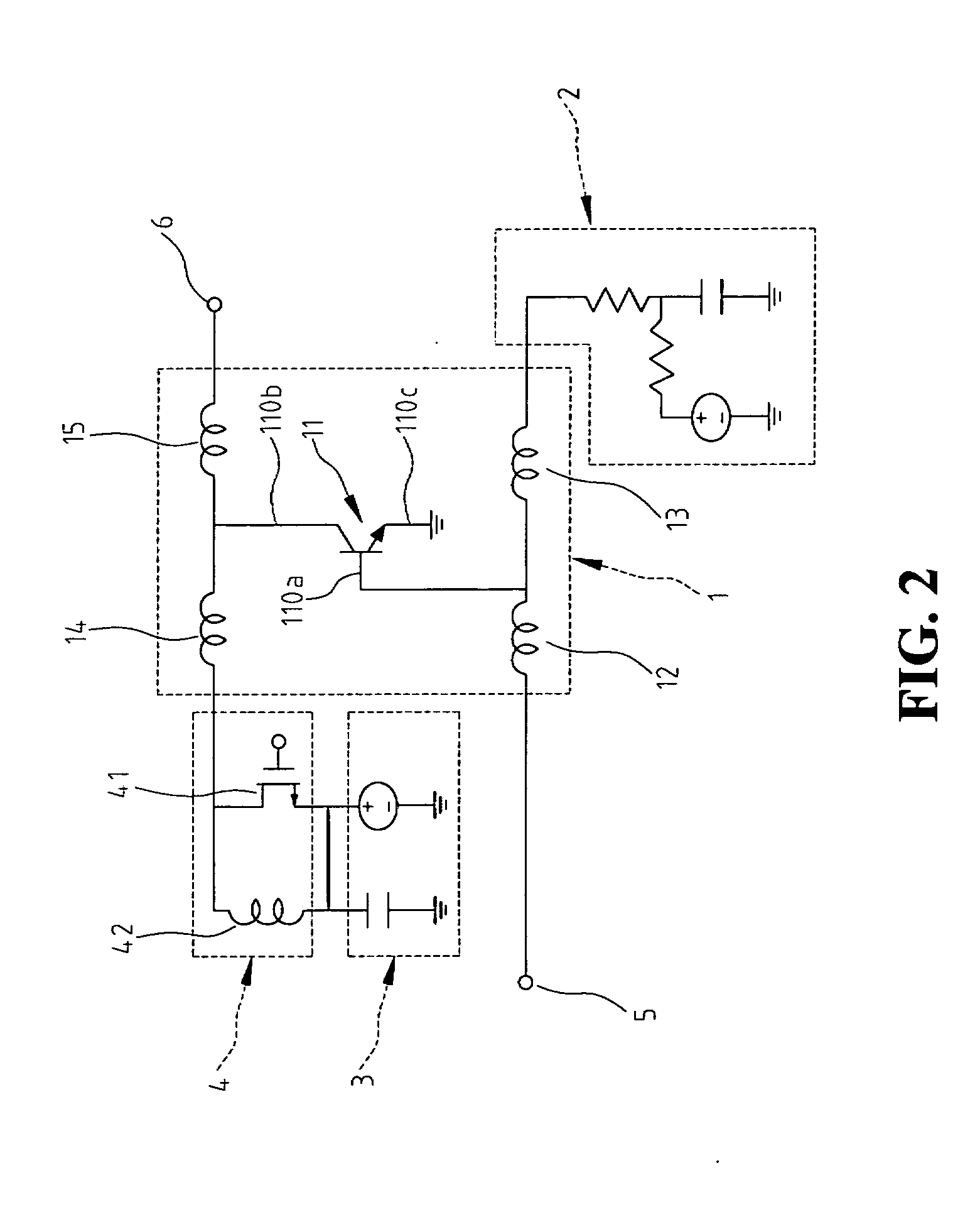
[0024]Referring to FIG. 3, a circuit diagram of the distributed amplifier according to the present invention is shown therein. In this embodiment, the active device 11 in the signal amplification unit 1 is composed of a plurality of sub-active devices, a first sub-active device 11a, a second sub-active device 11b and a third sub-active device 11a in the drawing. Although three sub-active devices are illustrated in the drawing, the sub-active devices may have any number greater than one, such as two and seven. In this case, a first inductor 17 and a second inductor 18 are connected between two adjacent sub-active devices 110a and 110b or 110b and 110c. The first active device 11a has an input terminal 110a electrically connected to the first external inductor 12 and an output terminal 110b electrically connected to the third external inductor 14. The second active device 11b has an input terminal 110a electrically connected to the second external inductor 13 and an output terminal 11...
third embodiment
[0025]Referring to FIG. 4, a circuit diagram of the distributed amplifier according to the present invention is shown therein. In this embodiment, a plurality of thus-constructed distributed amplifiers are coupled in series to form a distributed amplifier with multiple-stage amplifiers, in which a block capacitor 400 is provided between each two adjacent single stage distributed amplifiers 200, 300. It is to be noted that the block capacitor 400 may be implemented with at least a micro-stripe having an equivalent capacitance with respect thereto or at least a lumped device having an equivalent capacitance with respect thereto. In the drawing, the distributed amplifier is depicted as a two-stage form, but other stage number may also be contemplated. Herein, the two stages 200, 300 are termed as a first stage distributed amplifier 200 and a second stage distributed amplifier 300, respectively. Assuming now a RF input signal is fed into the distributed amplifier at the RF input termina...
PUM
 Abstract
Description
Claims
Application Information