Antenna Pattern And Electromagnetic-Wave Energy Processing Device Having The Same

a technology of electromagnetic wave energy processing and antenna pattern, which is applied in the direction of waveguide type devices, substantially flat resonant elements, resonance antennas, etc., can solve the problems of severe social problems, unsatisfactory clear display images, etc., and achieve clearer and more stable images, improve directivity, and improve image clarity

Active Publication Date: 2008-02-07
SHUHOU
View PDF8 Cites 7 Cited by
  • Summary
  • Abstract
  • Description
  • Claims
  • Application Information

AI Technical Summary

Benefits of technology

[0032]A conductor wire forming an antenna pattern according to the present invention is formed out of an aggregated wire consisting of mesh or continuously polygonal micro-image element lines or a parallel element wire. Accordingly, the antenna pattern can support a broad band of frequencies, and the directivity can be improved. In addition, due to an effect as a noise filter, a clearer image on a displa

Problems solved by technology

However, clearness of display images thereon is not always satisfactory.
On the other hand, electromagnetic waves propagated from various electromagneti

Method used


Image

  • Antenna Pattern And Electromagnetic-Wave Energy Processing Device Having The Same
  • Antenna Pattern And Electromagnetic-Wave Energy Processing Device Having The Same
  • Antenna Pattern And Electromagnetic-Wave Energy Processing Device Having The Same

Examples


example 1

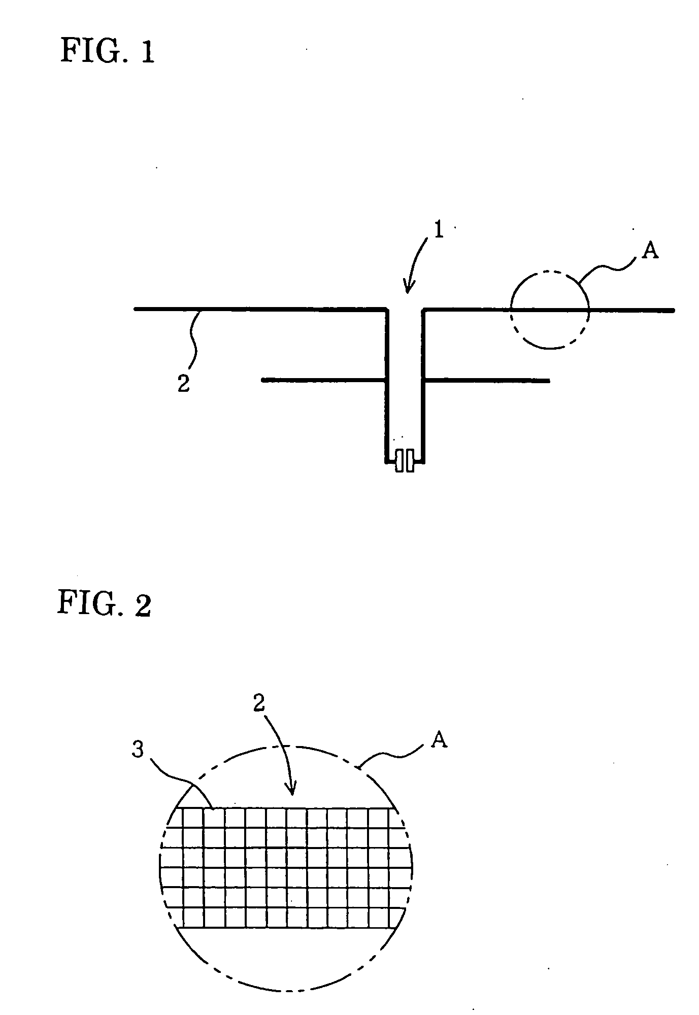
[0049]FIG. 1 is a diagram showing an antenna pattern in Example 1 of the present invention.

[0050]FIG. 2 is an enlarged reference diagram of a portion A in FIG. 1, showing an example where the aggregated wire consists of lattice type mesh micro-image element lines.

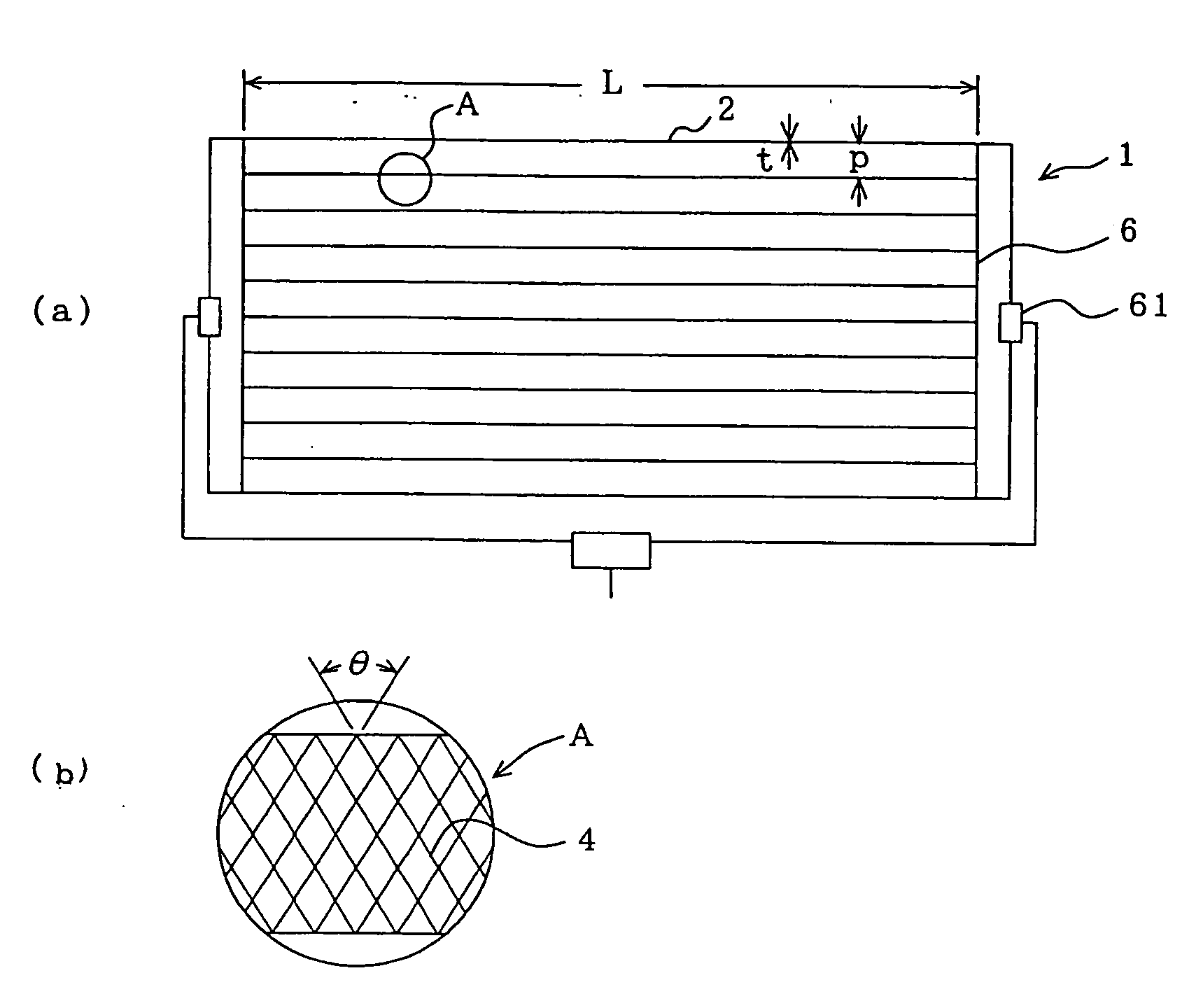
[0051]In the drawings, the reference numeral 1 represents an antenna pattern; 2, a conductor wire; and 3, mesh micro-image element lines.

[0052]The antenna pattern in Example 1 was formed to be 2 mm in width of a conductor wire, 39 cm in length of a long wire portion, 25 cm in length of a short wire portion and 3 cm in interval between the two wires, while the conductor wire was formed as an aggregated wire having a lattice type mesh pattern. The line width was set to be 20 μm and the line pitch interval was set to be 100 μm. The antenna pattern was printed by offset printing with synthetic ink mixed with Pd powder having an average particle size of 1 μm. Cu-plating about 1 μm thick was performed upon the printed surface by ...

example 2

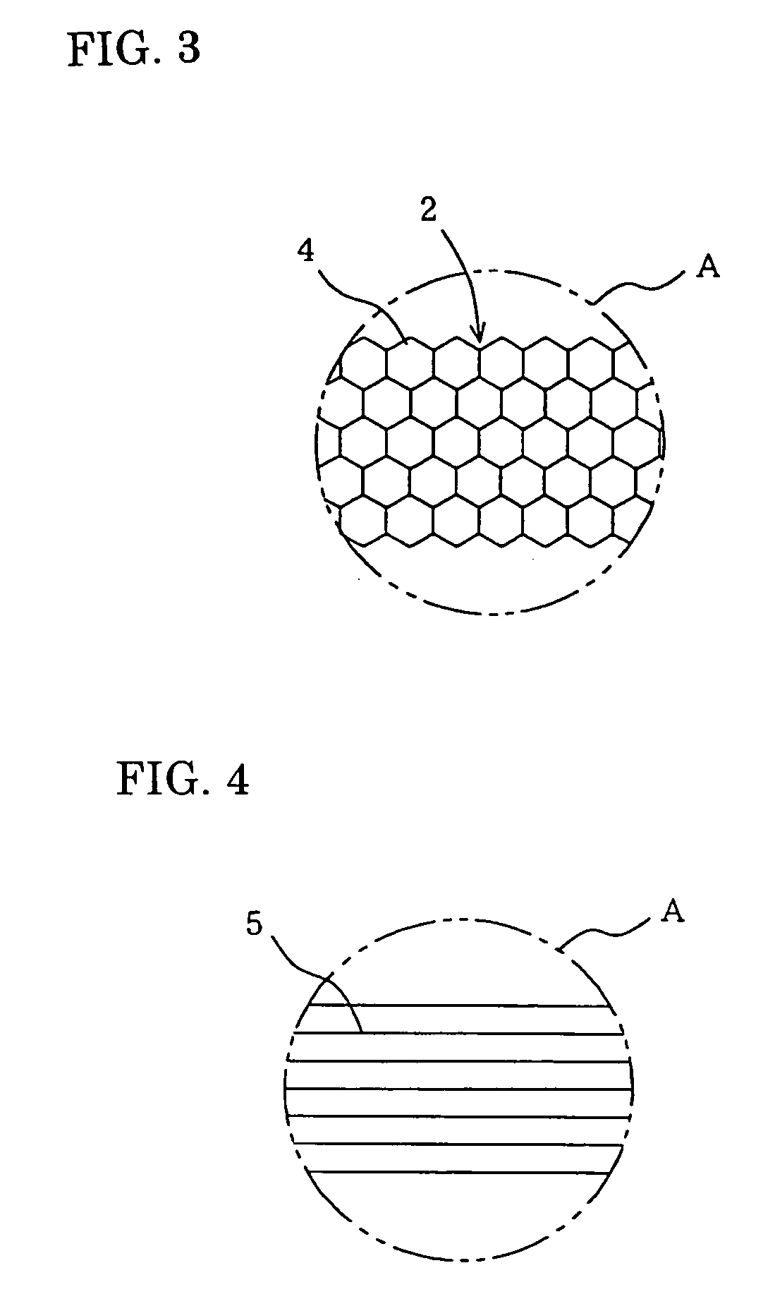
[0056]FIG. 3 is an enlarged reference diagram of a portion A in Example 2 of the present invention, showing an example where the aggregated wire consists of continuously polygonal micro-image element lines.

[0057]In the drawing, the reference numeral 4 represents a continuously polygonal micro-image element lines.

[0058]In the same manner as in Example 1, the antenna pattern in Example 2 was formed to be 2 mm in width of a conductor wire, 39 cm in length of a long wire portion, 25 cm in length of a short wire portion and 3 cm in interval between the two wires, while the conductor wire was formed as an aggregated wire having a lattice type mesh pattern. The line width was set to be 20 μm, and the pitch between opposite sides of each continuous polygonal shape was set to be 100 μm. The antenna pattern was printed by offset printing with synthetic ink mixed with Pd powder having an average particle size of 1 μm. Cu-plating about 1 μm thick was performed upon the printed surface by electr...

example 3

[0062]FIG. 4 is an enlarged reference diagram of a portion A in Example 3 of the present invention, showing an example where the aggregated wire consists of parallel aggregated lines.

[0063]In the drawing, the reference numeral 5 represents a parallel aggregated lines like a straight lines.

[0064]In the same manner as in Example 1, the antenna pattern in Example 3 was formed to be 2 mm in width of a conductor wire, 39 cm in length of a long wire portion, 25 cm in length of a short wire portion and 3 cm in interval between the two wires, while the conductor wire was formed as a parallel aggregated wire. The line width was set to be 20 μm, and the line pitch was set to be 100 μm. The antenna pattern was printed by offset printing with synthetic ink mixed with Pd powder having an average particle size of 1 μm. Cu-plating about 1 μm thick was performed upon the printed surface by electroless plating.

[0065]For the sake of comparison, an antenna pattern with the same pattern, in which the a...


PUM


Abstract

An antenna pattern having a broad band characteristic as to frequencies and having a wide directivity, and an electromagnetic wave energy processing device having the antenna pattern, particularly a sheet-like antenna or electromagnetic wave shielding filter. A conductor wire forming the antenna pattern comprises an aggregated wire consisting of mesh or continuously polygonal micro-image element lines or parallel element lines. The element lines are 5-300 μm in line width and 5-1,000 μm in line pitch interval, or the most preferably 5-30 μm in line width and 5-150 μm in line pitch interval. The element lines are printed with printing ink or paste material mixed with conductive powder. In accordance with necessity, pressure treatment or polishing treatment and/or conductive plating with aid of eletroless plating or directly without aid of eletroless plating are performed on the printed surface.

Description

TECHNICAL FIELD[0001]The present invention relates to an antenna pattern for use in a television set, a cellular phone or the like, and an electromagnetic-wave energy processing device having the antenna pattern, particularly a sheet-like antenna or electromagnetic wave shielding filter.BACKGROUND ART[0002]With the popularization of television sets or cellular phones, various antenna forms have been developed.[0003]However, clearness of display images thereon is not always satisfactory. There has been therefore a strong request for clearness of images on displays. In addition, receiving frequencies have been also made higher and higher from VHF (Very High Frequency to UHF Micro Wave. Antennas corresponding thereto have been therefore devised (for example, see Patent Document 1).[0004]As for antennas for displays for automobile use, antenna patterns provided in glass surfaces of rear portions of cars have been devised variously (for example, see Patent Document 2).[0005]On the other ...

Claims


Application Information

Patent Timeline
IPC IPC(8): H01Q1/36H01P11/00H01Q1/32H01Q1/38H01Q9/16H01Q9/28
CPCH01Q1/38H01Q1/364H01Q9/0407H01Q9/285
Inventor MURAOKA, KOUJI
Owner SHUHOU
Why Eureka
Try Eureka