Photoelectric conversion sensor

a technology of photoelectric conversion and sensor, which is applied in the direction of instruments, radiation controlled devices, optical radiation measurement, etc., can solve the problems of difficult to increase the size of the semiconductor substrate, difficult to reduce the cost, and large number of man-hours for the production of such photoelectric conversion pixels, so as to reduce the variation in thickness, reduce the height difference between the electrodes, and reduce the possibility of wire breakage on the substrate

Inactive Publication Date: 2008-02-14
PANASONIC CORP
View PDF9 Cites 23 Cited by
  • Summary
  • Abstract
  • Description
  • Claims
  • Application Information

AI Technical Summary

Benefits of technology

[0018]As described above, an optical filter is provided on a light transmissive substrate separate from organic photoelectric conversion pixel part. It is thus possible to reduce the height difference between the electrodes of the organic photoelectric conversion pixel part and the substrate thus reducing possible wire break in a wire on the substrate.
[0019]It is made easy to reduce variations in thickness between the organic photoelectric conversion pixels thus upgrading the data reading quality.

Problems solved by technology

Production of such photoelectric conversion pixels requires a large-scale semiconductor process with a very large number of man-hours.
Further, it is difficult to increase the size of a semiconductor substrate.
As a result, a related art photoelectric conversion sensor is accompanied by a problem that cost reduction is difficult.

Method used


Image

  • Photoelectric conversion sensor
  • Photoelectric conversion sensor
  • Photoelectric conversion sensor

Examples


embodiment 1

[0035]A photoelectric conversion sensor, a photoelectric conversion unit or an image reader using the photoelectric conversion sensor or photoelectric conversion unit is applicable to a device, such as a facsimile or a scanner, for converting an image of a subject of imaging to an electric signal to obtain image data.

[0036]An image reader moves a photoelectric conversion unit and an original relatively from each other and creates image data based on an electric signal outputted from the photoelectric conversion unit while displacing the imaging position of an original. The image reader may be of a reflective type or a transmission type.

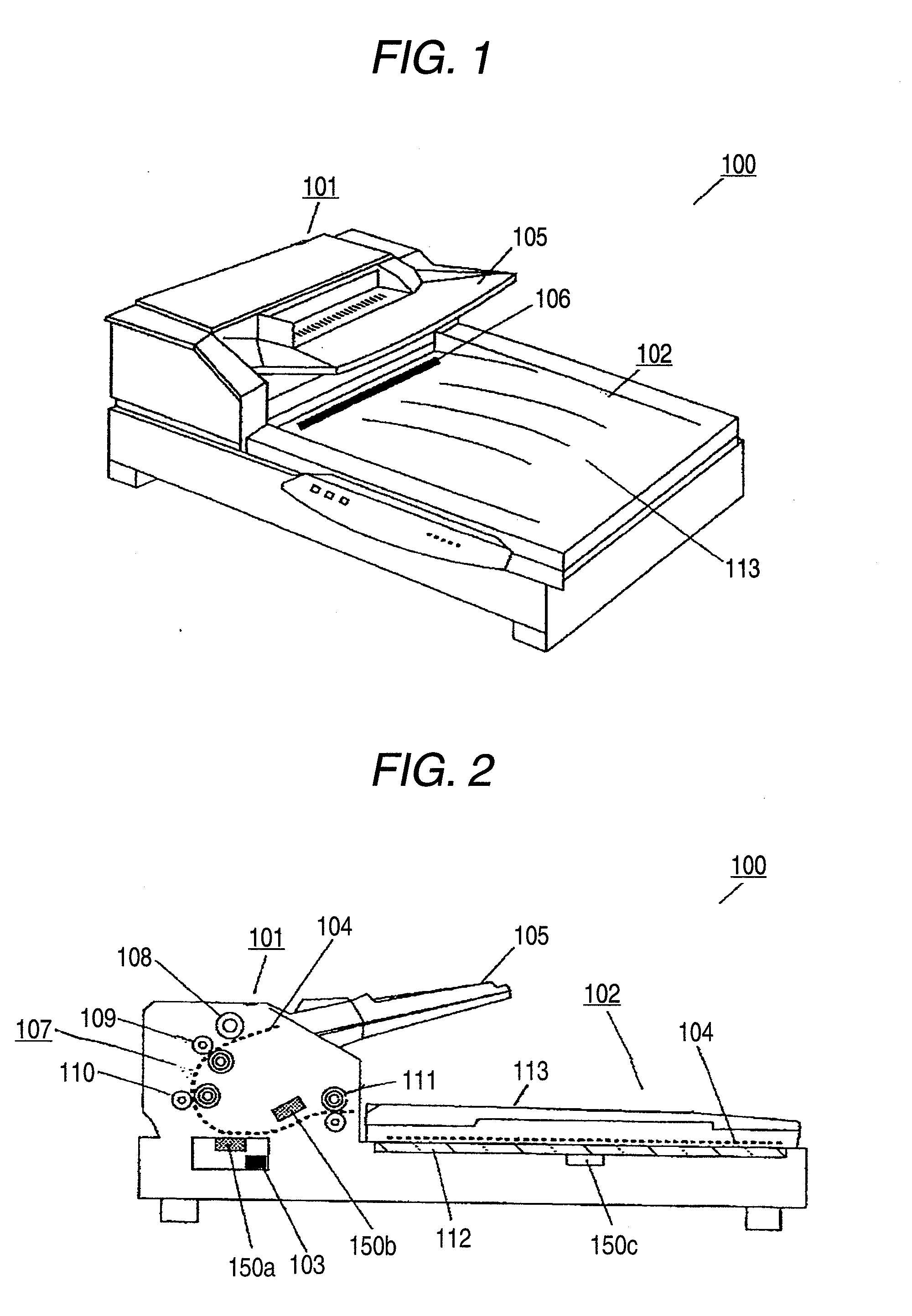
[0037]FIG. 1 is a perspective view showing the external appearance of an image reader according to Embodiment 1. FIG. 2 is a cross-sectional view showing the internal structure of the image reader according to Embodiment 1 and shows in this case a scanner as an example of image reader.

[0038]As shown in FIGS. 1 and 2, an image reader 100 reads the info...

embodiment 2

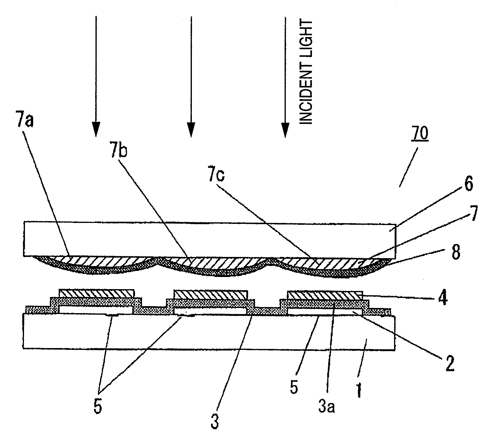
[0082]FIG. 5 is a cross-sectional view schematically showing a photoelectric conversion sensor according to Embodiment 2.

[0083]As shown in FIG. 5, a photoelectric conversion sensor 71 has a substrate 1 on which a plurality of organic photoelectric conversion pixel parts 5 are mounted and a light transmissive substrate 6 on which an optical filter 7 is mounted bonded together with a moisture-resistant resin 10. That is, FIG. 5 shows the moisture-resistant resin 10 as an example of a support member according to Embodiment 1.

[0084]The moisture-resistant resin 10 is formed so as to be bonded to the substrate 1 outside an area in a plan view where the plurality of organic photoelectric conversion pixel parts 5 are arranged and so as to be bonded to the light transmissive substrate 6 outside an area in plan view where the optical filter 7 is arranged. The moisture-resistant resin layer 10 bonds together the substrate 1 and the light transmissive substrate 6 (refer to FIGS. 11 and 12 below...

embodiment 3

[0092]FIG. 6 is a cross-sectional view schematically showing a photoelectric conversion sensor according to Embodiment 2.

[0093]In a photoelectric conversion sensor 72 shown in FIG. 6, a moisture-resistant resin layer 10a is formed so as to cover each organic photoelectric conversion pixel part 5 and the moisture-resistant resin layer 10a is used to bond together a substrate 1 and a light transmissive substrate 6. The moisture-resistant resin layer 10a has light transmission properties.

[0094]The photoelectric conversion sensor 72 having such a structure delivers the same technical effects as the photoelectric conversion sensor 71 described in Embodiment 2 and is more advantageous in that it is made easy to form the moisture-resistant resin layer 10a.

[0095]Same as the moisture-resistant resin layer 10 described in Embodiment 2, the moisture-resistant resin layer 10a may be formed by a photo-setting or thermosetting resin. Extreme care should be taken to prevent degradation or destruc...


PUM


Abstract

A photoelectric conversion sensor according to the invention comprises: a substrate; a plurality of organic photoelectric conversion pixel parts arranged on the substrate for converting incident light to an electric signal; a light transmissive substrate for transmitting incident light; an optical filter arranged on the light transmissive substrate for limiting the wavelength range of incident light to the plurality of organic photoelectric conversion pixel parts; and a support part for supporting the substrate and the light transmissive substrate in a state where the organic photoelectric conversion pixel parts are separated from the optical filter.

Description

BACKGROUND[0001]1. Field of the Invention[0002]The present invention relates to a photoelectric conversion sensor for converting an incident light from a subject of imaging such as an original by using organic photoelectric conversion pixels.[0003]2. Description of the Related Art[0004]A photoelectric conversion sensor for converting reflect light from an original or direct light to an electric signal is widely used in a device such as a facsimile or a scanner. The photoelectric conversion sensor comprises a plurality of photoelectric conversion pixels for generating an electric signal having a magnitude corresponding to the intensity of an incident light and an optical system for guiding reflected light from a readout object or direct light to the photoelectric conversion pixels. The photoelectric conversion pixels are mainly photodiodes, photoconductors or phototransistors using inorganic semiconductors or their application components.[0005]Production of such photoelectric convers...

Claims


Application Information

Patent Timeline
Patent Type & Authority Applications(United States)
IPC IPC(8): H01L27/00G01J1/04H01L27/14H01L27/146H01L31/10H04N1/028H04N5/335H04N5/369
CPCB82Y10/00H01L51/0047H01L27/307H10K39/32H10K85/215
Inventor KOMATSU, TAKAHIROMIZUSAKI, MASAKAZUKANEKO, SHINICHIROINOUE, MASAHIROKITADA, TAKASHI
Owner PANASONIC CORP
Why Eureka
Try Eureka