Liquid crystal device and electronic apparatus

a liquid crystal device and electronic equipment technology, applied in non-linear optics, instruments, optics, etc., can solve the problems of difficult manufacturing of thin electronic equipment, general thickness, and difficulty in forming thin electronic equipment, and achieve the effect of reducing the overall thickness of the liquid crystal device and reducing the thickness

Inactive Publication Date: 2008-02-14
JAPAN DISPLAY WEST
View PDF6 Cites 18 Cited by
  • Summary
  • Abstract
  • Description
  • Claims
  • Application Information

AI Technical Summary

Benefits of technology

[0022]According to another aspect of the invention, an electronic apparatus includes the liquid crystal device having the above configurations. The liquid crystal device forms images on the surface of the first substrate using the first sub-pixels and on the surface of the second substrate using the second sub-pixels. Therefore, double-sided display is possible by means of one liquid crystal panel consisting of two substrates of the first substrate and the second substrate. As a result, it is possible to reduce the overall thickness of a liquid crystal device, as compared with liquid crystal devices that display images on both sides of the front and rear surfaces using two liquid crystal panels in the related art. Therefore, the electronic apparatus according to another aspect of the invention including the liquid crystal device is also reduced in thickness.

Problems solved by technology

However, the liquid crystal devices disclosed in JP-A-2005-77429 and JP-A-2005-78802 each have two liquid crystal panels, so that they are generally thick compared with other liquid crystal devices that display images using only one liquid crystal panel.
Therefore, it was difficult to manufacture thin electronic apparatuses each using the liquid crystal devices with two liquid crystal panels.
In this case, the components formed on the first substrate and the second substrate are complicated in structure, which makes manufacturing of the liquid crystal device difficult and causes poor operation of the liquid crystal device.

Method used


Image

  • Liquid crystal device and electronic apparatus
  • Liquid crystal device and electronic apparatus
  • Liquid crystal device and electronic apparatus

Examples


first embodiment

of Liquid Crystal Device

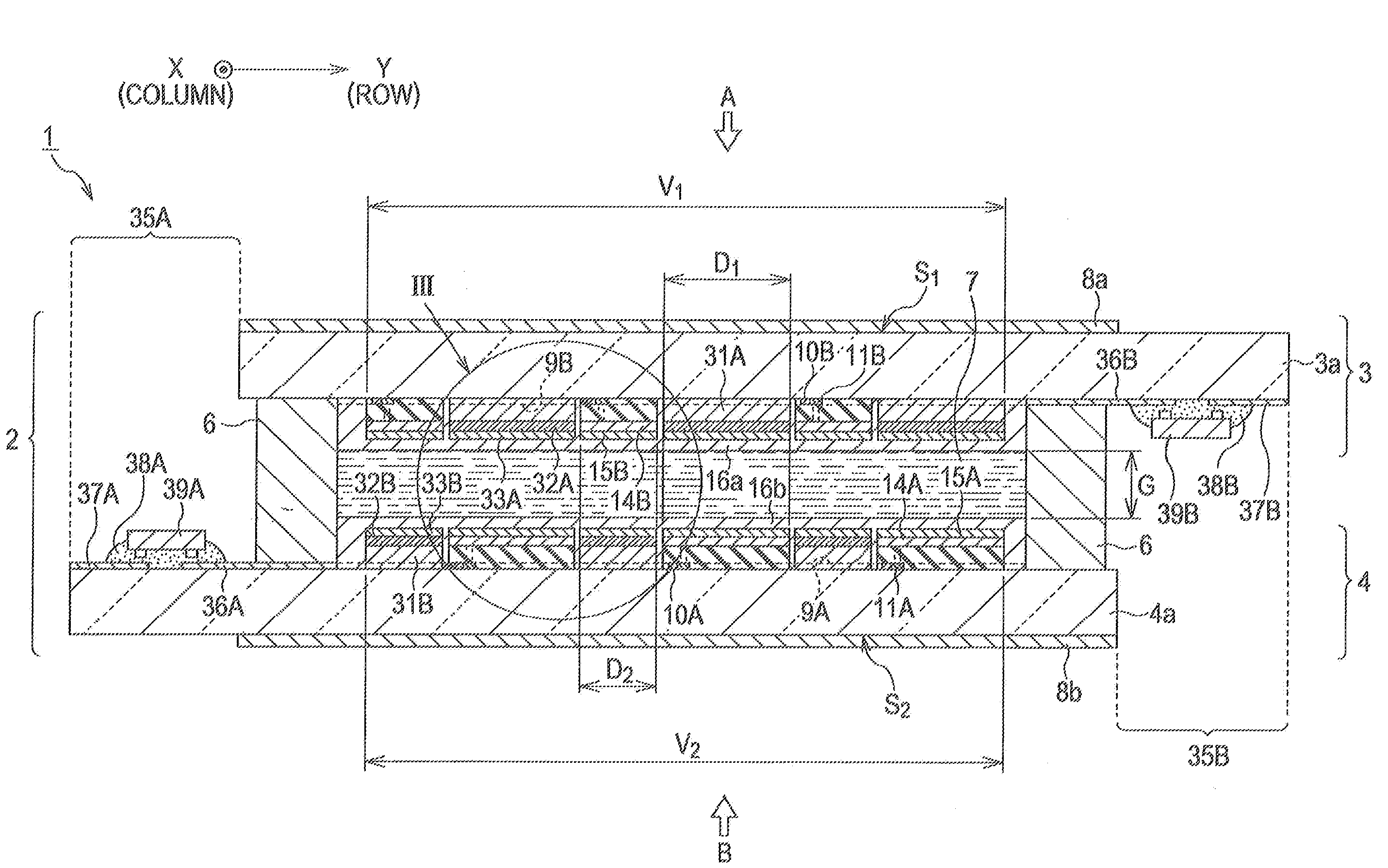
[0038]Preferred embodiments of the invention are described hereafter by exemplifying a reflective liquid crystal device to which the invention is applied that is capable of displaying colors by driving TFTs (Thin Film Transistor) as a liquid crystal device. Further, in this embodiment, the invention is applied to a liquid crystal device with amorphous silicon TFT elements of an H-channel-type single gate structure, as TFT elements. The invention is not limited to the embodiments. Further, a plurality of components may be shown having dimensions different from their actual dimensions to aid understanding of figures referred to in relation to the following description.

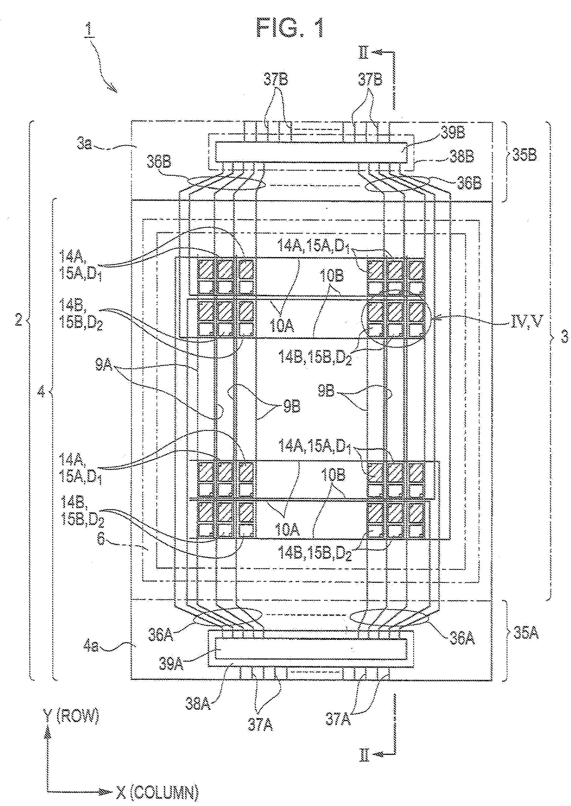
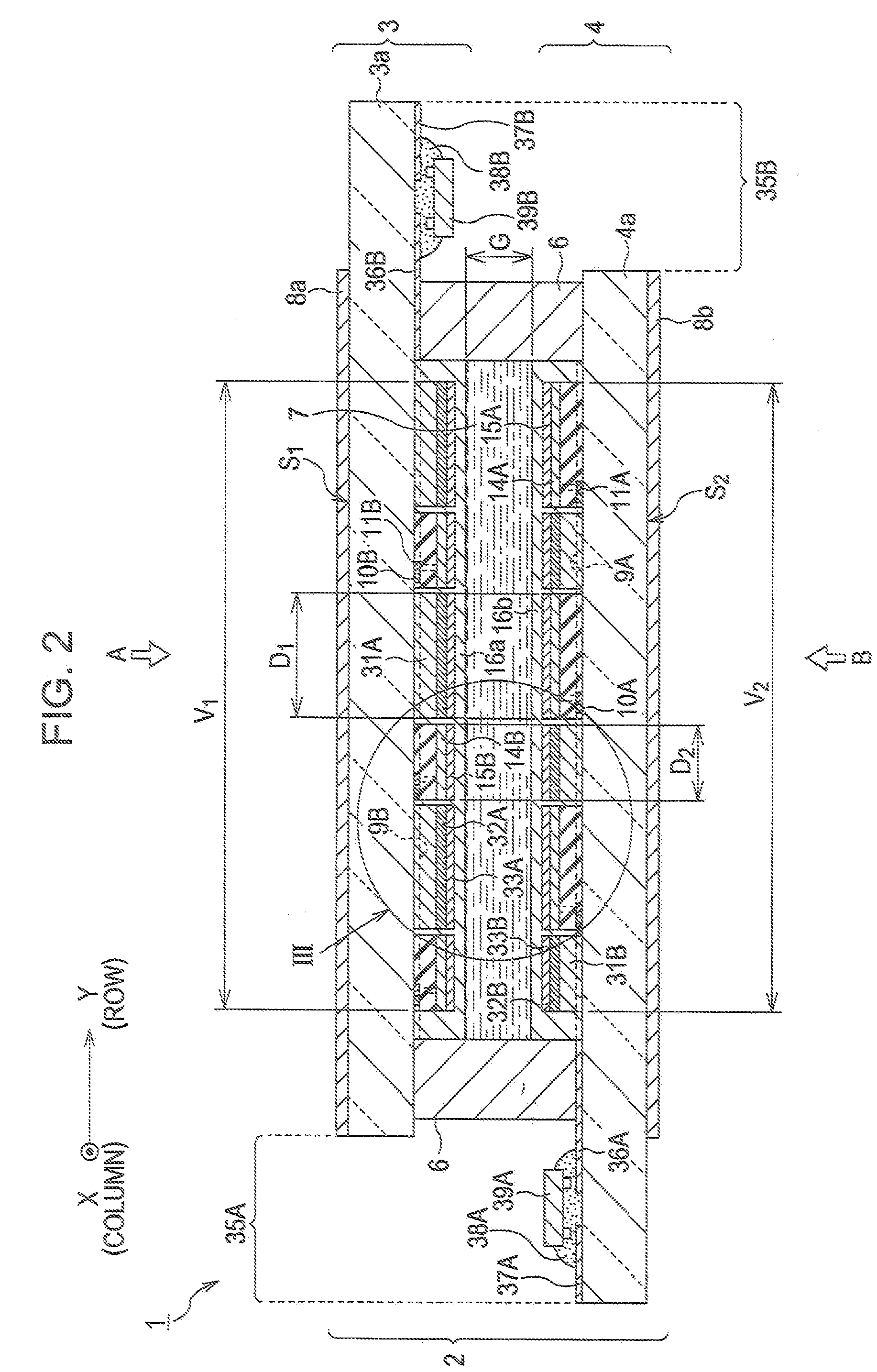
[0039]FIG. 1 is a plan view showing the structure of a liquid crystal device according to an embodiment of the invention. FIG. 2 is a cross-sectional view of the liquid crystal device taken along the line II-II of FIG. 1. FIG. 3 is an enlarged view of a portion indicated by an arrow III of FIG. 2....

second embodiment

of Liquid Crystal Device

[0092]Next, a liquid crystal device according to another embodiment of the invention is described below. FIG. 7 is a plan view illustrating the structure of a liquid crystal device 51 according to this embodiment. FIG. 8 is a cross-sectional view illustrating the structure, taken along the line VIII-VIII of FIG. 7. FIG. 9 is an enlarge view of the portion indicated by the arrow IX of FIG. 8. FIGS. 10 and 11 are enlarged views of the portion indicated by the arrow X, XI of FIG. 7. Further, FIG. 10 shows the main plan structure of a substrate 54, seen from the direction of arrow A of FIG. 9. FIG. 11 shows the main plan structure of a substrate 53, seen from the direction of arrow B of FIG. 9.

[0093]The configuration of a liquid crystal device 51 of FIG. 7 according to this embodiment is the same as the liquid crystal device 1 shown in FIG. 1, except for the arrangement of the first sub-pixels D1 and the second sub-pixels B2 in the region surrounded the sealing m...


PUM

PropertyMeasurementUnit
sizeaaaaaaaaaa
colorsaaaaaaaaaa
thicknessaaaaaaaaaa

Abstract

A liquid crystal device includes a first substrate and a second substrate that face each other, a liquid crystal layer that is interposed between the first substrate and the second substrate, light reflecting films that are selectively provided on the side facing the liquid crystal layer of the first substrate and reflect light entering from the second substrate, light reflecting films that are selectively provided on the side facing the liquid crystal layer of the second substrate, corresponding to the regions of the first substrate where the light reflecting films are not provided and reflect light entering from the first substrate, transmissive electrodes that are selectively provided in the regions of the side facing the liquid crystal layer of the first substrate where the light reflecting films are not provided, and transmissive electrodes that are selectively provided in the regions of the side facing the liquid crystal layer of the second substrate where the light reflecting films are not provided.

Description

BACKGROUND[0001]1. Technical Field[0002]The present invention relates to a liquid crystal device that forms images by modulating light passing through a liquid crystal layer. Further, the invention relates to an electronic apparatus using the liquid crystal device.[0003]2. Related Art[0004]Liquid crystal devices are now in wide use in electronic apparatuses, such as mobile phones and portable information terminals, as display portions that visually display a variety of information relating to operation of the electronic apparatuses. Such a liquid crystal device generally has a liquid crystal panel formed by disposing a liquid crystal layer between a pair of substrates facing each other and displays images, such as characters, numbers, and figures, on the outer surface of the later one of the substrates in the travel direction of light by modulating light passing through the liquid crystal panel for each of a plurality of sub-pixels.[0005]Liquid crystal devices with two liquid crysta...

Claims


Application Information

Patent Timeline
Patent Type & Authority Applications(United States)
IPC IPC(8): G02F1/1335
CPCG02F2001/133342G02F1/133555G02F1/133342
Inventor OTAKE, TOSHIHIRO
Owner JAPAN DISPLAY WEST
Why Eureka
Try Eureka