Electro-optical device, method for manufacturing electro-optical device, and electronic apparatus
- Summary
- Abstract
- Description
- Claims
- Application Information
AI Technical Summary
Benefits of technology
Problems solved by technology
Method used
Image

Examples
first embodiment
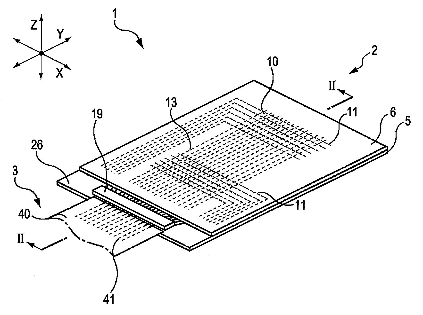
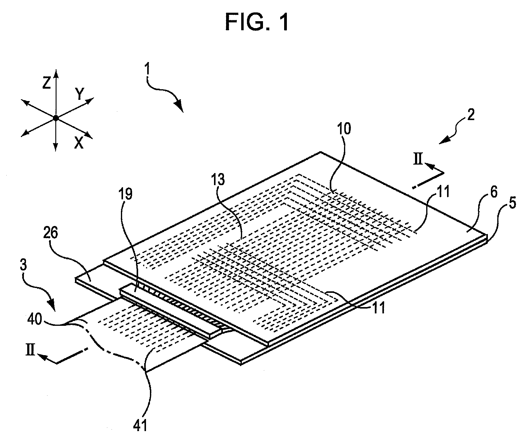
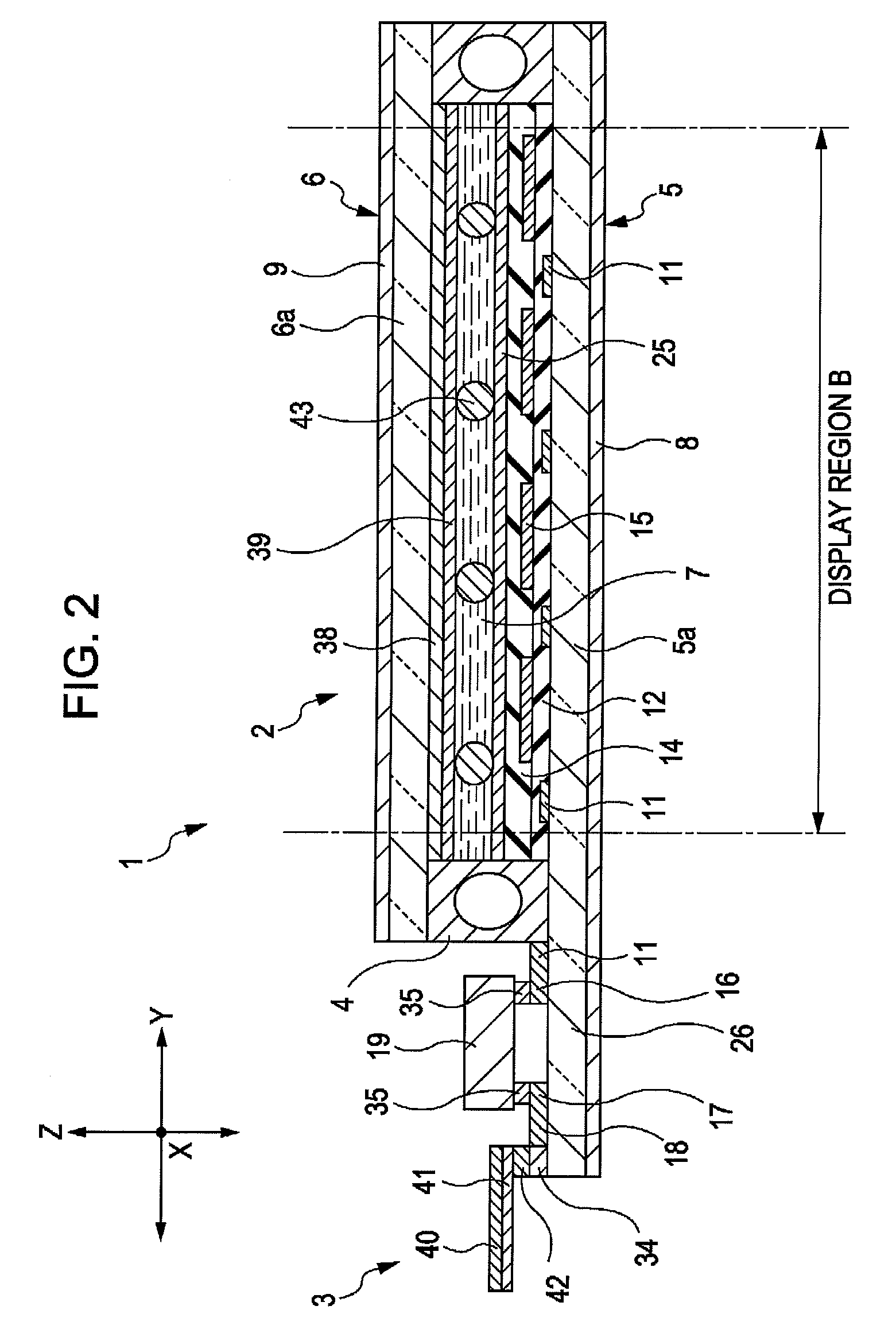
[0057]FIG. 1 shows an electro-optical device 1 according to a first embodiment of the present invention in perspective view. FIG. 2 shows the electro-optical device in sectional view taken along the line II-II of FIG. 1.
[0058]With reference to FIG. 1, the electro-optical device 1 includes a liquid crystal panel 2 and a flexible board 3 electrically connected to the liquid crystal panel 2. The electro-optical device 1 may further include a lighting unit such as a backlight and ancillary components, which are not shown, as required.
[0059]With reference to FIG. 2, the liquid crystal panel 2 includes a sealing member 4, a first substrate 5, a second substrate 6 bonded to the first substrate 5 with the sealing member 4 disposed therebetween, and a twisted nematic (TN) liquid crystal 7 disposed between the first and second substrates 5 and 6 in a sealed manner.
[0060]The first and second substrates 5 and 6 include a first base member 5a and a second base member 6a, respectively. The first ...
second embodiment
[0133]An electro-optical device according to a second embodiment of the present invention will now be described. The electro-optical device of this embodiment is different from that of the first embodiment in that contact sections are not disposed on center portions of first metal layers but are disposed on end portions of the first metal layers. Components common to those described in the first embodiment have the same reference numerals and will not be described in detail. A method for manufacturing the electro-optical device of this embodiment is substantially the same as that for manufacturing the electro-optical device 1 of the first embodiment and will not be described in detail.
[0134]FIG. 14 shows one of gate output connection terminals 116a disposed in the electro-optical device in plan view. FIG. 15 shows the gate output connection terminal 116a in sectional view taken along the line XV-XV of FIG. 14. FIG. 16 shows one of source output connection terminals 116b disposed in ...
third embodiment
[0164]An electro-optical device according to a third embodiment of the present invention will now be described. The electro-optical device of this embodiment is different from that of the first embodiment in that contact sections are not disposed on center portions of first metal layers disposed in output connection terminals but are disposed on end portions of the first metal layers that are located on the leading side of the first metal layers.
[0165]FIG. 18 shows one of gate output connection terminals 216a disposed in the electro-optical device in plan view. FIG. 19 shows the gate output connection terminal 216a in sectional view taken along the line XIX-XIX of FIG. 18.
[0166]With reference to FIGS. 18 and 19, the gate output connection terminals 216a each include a first gate metal layer 27a which is disposed on a first base member 5a so as to be located in a mount region C and which has substantially a rectangular shape. The first gate metal layer 27a is connected to a side (the...
PUM
 Abstract
Description
Claims
Application Information
 - Generate Ideas
- Intellectual Property
- Life Sciences
- Materials
- Tech Scout
- Unparalleled Data Quality
- Higher Quality Content
- 60% Fewer Hallucinations
Browse by: Latest US Patents, China's latest patents, Technical Efficacy Thesaurus, Application Domain, Technology Topic, Popular Technical Reports.
© 2025 PatSnap. All rights reserved.Legal|Privacy policy|Modern Slavery Act Transparency Statement|Sitemap|About US| Contact US: help@patsnap.com