Light-emitting device, method of fabricating the same, and electronic apparatus

a technology of light-emitting devices and electronic devices, which is applied in the direction of identification means, instruments, diffusing elements, etc., can solve the problems of difficult planarization process of forming a planarization layer and the like, complicated processes, and inability to obtain directive scattering effects, etc., and achieves high-visibility display

Inactive Publication Date: 2008-02-21
SEIKO EPSON CORP
View PDF9 Cites 40 Cited by
  • Summary
  • Abstract
  • Description
  • Claims
  • Application Information

AI Technical Summary

Benefits of technology

[0027]According to another aspect of the invention, there is provided an electronic apparatus including the light-emitting device. It is possible for the electronic apparatus to achieve a highly visible display by the use of the light-emitting device.

Problems solved by technology

According to these known technologies, complicated processes are needed to form a microscopic structure and planarize an upper portion of the structure.
However, it becomes a structure that visible light is not directively scattered, so there is a case that the directive scattering effect can not be obtained.
When the height between the convex top portion and the concave bottom portion is 500 nm or more, there is a case that a planarization process of forming a planarization layer and the like becomes difficult.
When the waveform structure occupies less than 30% of the total area of the interface between the thin films, there is a case that light can not be sufficiently scattered.

Method used


Image

  • Light-emitting device, method of fabricating the same, and electronic apparatus
  • Light-emitting device, method of fabricating the same, and electronic apparatus
  • Light-emitting device, method of fabricating the same, and electronic apparatus

Examples


first embodiment

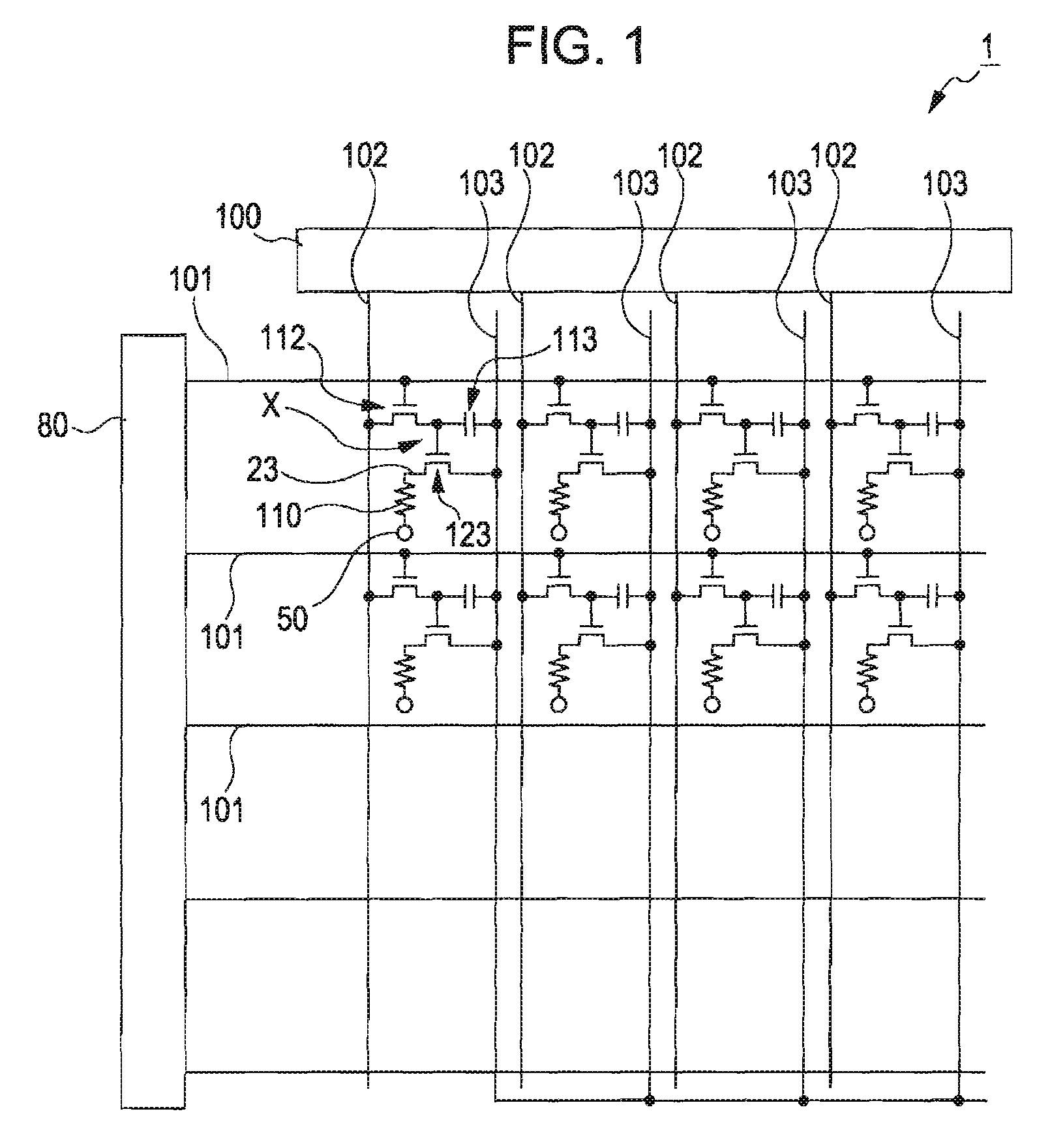
[0081]Next, a structure of a unit pixel group of the organic EL element with respect to a first embodiment of the organic EL element constituting an organic EL panel 1 will be described with reference to FIG. 3.

[0082]In FIG. 3, the pixel electrodes 23, the light-emitting layers 110, and the negative electrodes 50 constituting a part of the organic EL element corresponding to a pixel will be described in detail, and the driving TFT 123 is connected to the pixel electrodes 23. Additionally, the pixel electrodes 23 constituting the organic EL element are each formed for a red pixel XR, a green pixel XG, and a blue pixel XB. As shown in FIG. 1, each pixel is driven by the driving TFT 123.

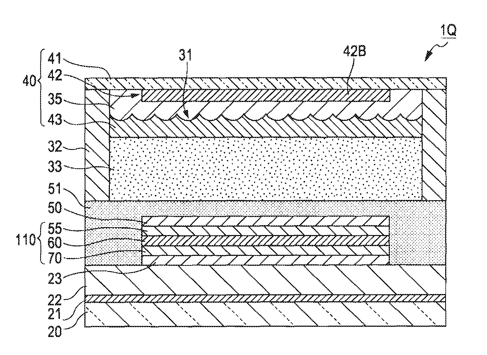
[0083]As shown in FIG. 3, a unit pixel group Px of the organic EL element (an organic EL device) 1A has the light-emitting layers 110 which are interposed between the pixel electrodes 23 and the negative electrodes 50 on a substrate 20. In addition, a color filter substrate 40 is formed opposite the sub...

second embodiment

[0111]Next, a structure of a unit pixel group of the organic EL element with respect to a second embodiment of the organic EL element constituting an organic EL panel 1 will be described with reference to FIG. 13.

[0112]FIG. 13 is a diagram corresponding to FIG. 3 showing the first embodiment of the organic EL element. About the same reference numerals and signs as those shown in FIG. 3, they are formed of the same configuration and member unless there are specific explanations.

[0113]In an organic EL element 1B according to the second embodiment, a configuration of the color filter substrate 40 is different from that of the organic EL element 1A according to the first embodiment. Specifically, the color filter substrate 40 includes the substrate 41 which is formed of a transparent member such as glass, the color filter layers 42 (42B, 42G, and 42R) which are formed on the substrate 41, a directive scattering layer 35 which is formed so as to cover the color filter layers 42, and the ...

third embodiment

[0115]Next, a structure of a unit pixel group of a organic EL element with respect to a third embodiment of the organic EL element constituting the organic EL panel 1 will be described with reference to FIG. 14.

[0116]FIG. 14 is a diagram corresponding to FIG. 3 showing the first embodiment of the organic EL element. About the same reference numerals and signs as those shown in FIG. 3, they are formed of the same configuration and member unless there are specific explanations.

[0117]In an organic EL element 1C according to the third embodiment, a configuration of the color filter substrate 40 is different from that of the organic EL element 1A according to the first embodiment. Specifically, the color filter substrate 40 includes a substrate 41 which is formed of the transparent member such as a glass material, the color filter layers 42 (42B, 42G, and 42R) which are formed on the substrate 41, the overcoat layer 43 which is formed so as to cover the color filter layer 42, and a direc...


PUM


Abstract

A light-emitting device is provided in which a plurality of thin films including a light-emitting layer are stacked. The light-emitting device includes a waveform structure having a directive scattering function in one interface between the thin films.

Description

BACKGROUND[0001]1. Technical Field[0002]The present invention relates to a light-emitting device, a method of fabricating the same, and an electronic apparatus.[0003]2. Related Art[0004]Light-emitting devices such as organic electro-luminescence devices (hereinafter, referred to organic EL devices) are being used as display devices for electronic apparatuses such as cellular phones, personal computers, and PDAs (Personal Digital Assistants) and exposure heads in image forming devices such as digital copy machines and printers. An example of a light-emitting device is one having a multi-layered structure formed by stacking a plurality of thin films with a variety of refractive indexes including a light-emitting layer.[0005]The refractive index of the light-emitting layer is different in accordance with a material, but it is generally in the range of 1.55 to 2.3 or so at 550 nm and is larger than those of air (n=1.0) and a glass material (n=1.5). Accordingly, light emitted from a laye...

Claims


Application Information

Patent Timeline
Patent Type & Authority Applications(United States)
IPC IPC(8): H01L21/00H01L33/00G02B5/02G09F9/30H01L27/32H01L51/50H05B33/02H05B33/10H05B33/14
CPCH01L27/3211H01L51/5268H01L51/5237H01L27/322H10K59/35H10K59/38H10K50/841H10K50/844H10K50/854H05B33/20H05B33/22
Inventor WANO, HIROMI
Owner SEIKO EPSON CORP
Why Eureka
Try Eureka