Thin-film transistor and fabrication method thereof

a thin film transistor and fabrication method technology, applied in the direction of transistors, semiconductor devices, electrical equipment, etc., can solve the problems of inability to extend the length of the gate (i.e. tft channel resolution) to several micrometers and less, and the size of the high-resolution electronic device is too large, so as to achieve the effect of fabricating an electronic devi

Inactive Publication Date: 2008-02-21
IND TECH RES INST
View PDF4 Cites 6 Cited by
  • Summary
  • Abstract
  • Description
  • Claims
  • Application Information

AI Technical Summary

Benefits of technology

[0013]Another object of the invention is to provide a TFT, wherein the central part of the coffee ring film is removed by etching to form an isolated line and reduce the width of the line by a controlled etching rate. In addition, the invention further dispenses an active material having solubility of solution on the micro-line structure of the coffee ring ridge. The active material can slightly etch the coffee ring ridge into a gradient concentration of the ridge.

Problems solved by technology

These technologies, however, are unable to extend the length of a gate (i.e. TFT channel resolution) to several micrometers and less.
In general, the diameter of the drop on the substrate is from several tens to several hundreds of micrometers, and is thus too large for high resolution electronic devices.
Because there are no isolated lines formed by the described technology, it cannot be used for fabricating an electronic device.
The disadvantages of this method include an additional cost for lift-off process.
At the same time, lift-off processes damaged the surfaces of the source / drain electrodes.

Method used


Image

  • Thin-film transistor and fabrication method thereof
  • Thin-film transistor and fabrication method thereof
  • Thin-film transistor and fabrication method thereof

Examples


first embodiment

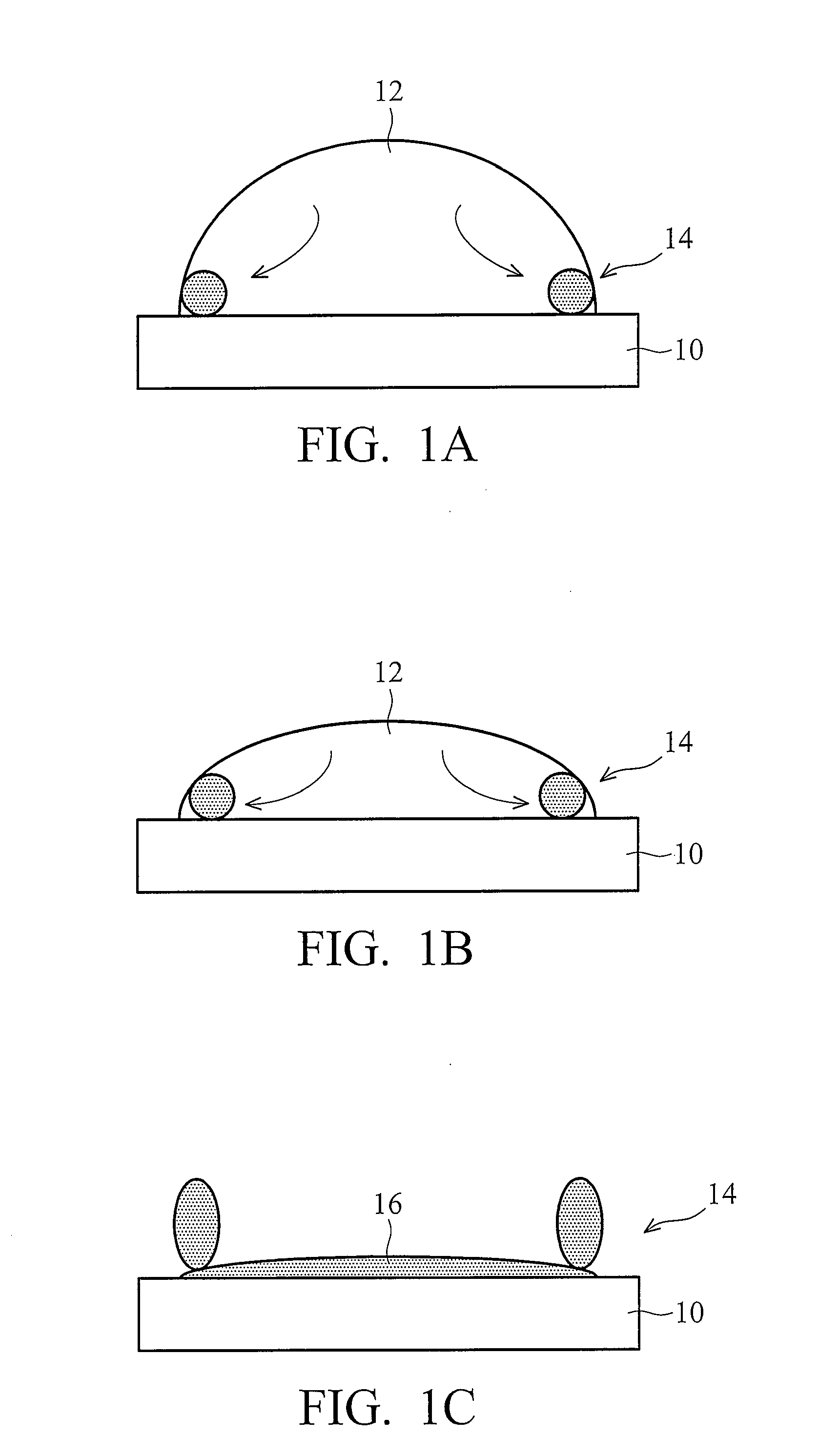
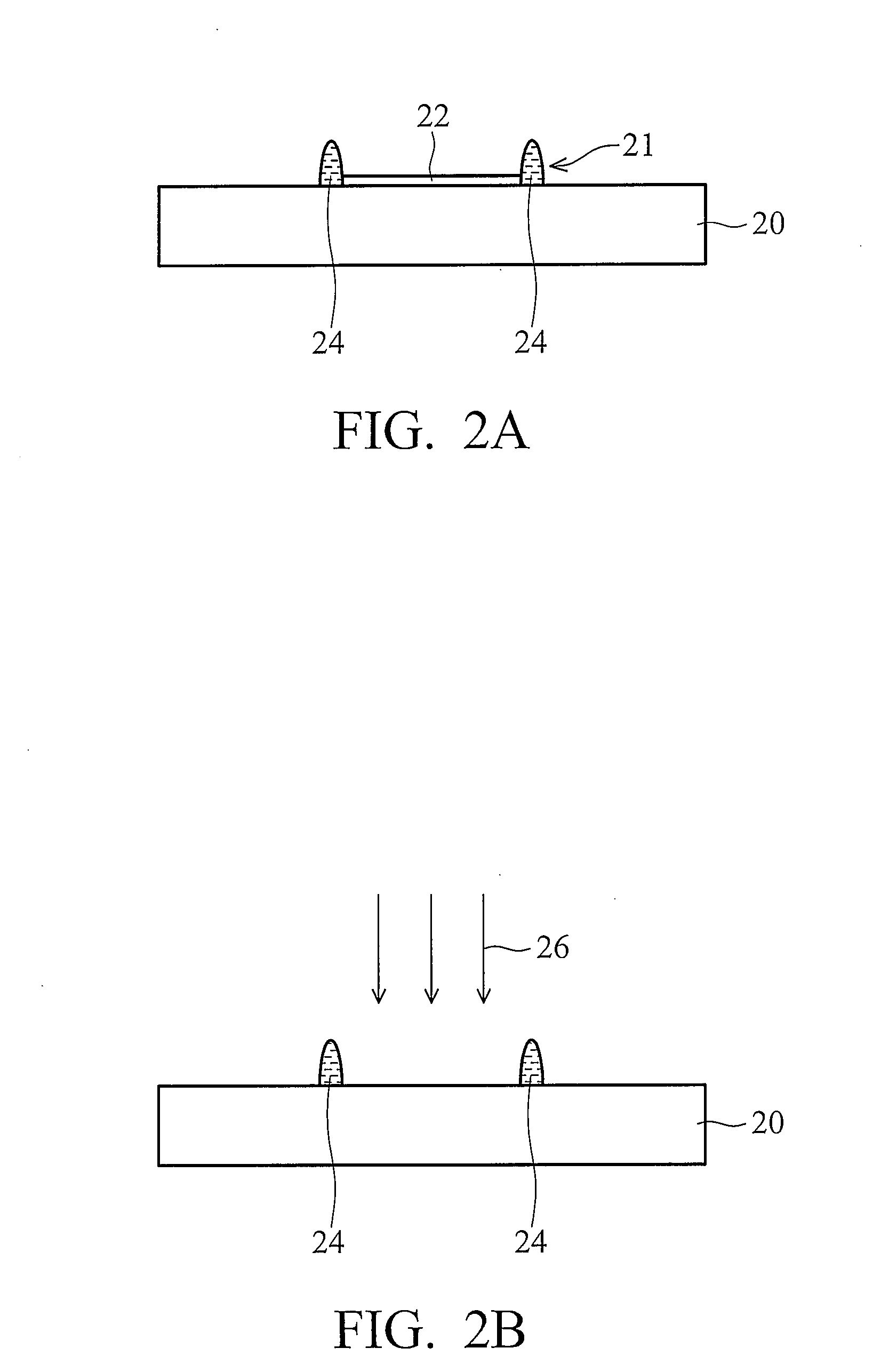
[0027]The cross sections of fabrication steps of the invention are shown in FIGS. 2A-2F. Referring to FIG. 2A, a substrate 20, such as glass or plastic substrate, is first provided. A semiconductor material solution is inkjet printed by a sprinkle-nozzle on the substrate 20 into a dot or a line shape, and then dried into a coffee ring film 21. The semiconductor material may be, but is not limited to, poly-(3-hexylthiophene) (P3HT) or poly-9(9dioctylfluorene-co-bithiophene) (F8T2). The semiconductor material is dissolved in a solvent into a solution for inkjet printing. The solvent includes watery liquid or an oily liquid such as xylene.

[0028]Referring to FIG. 2B, a central part 22 of the coffee ring film 21 is removed by a surface micro-etching method, and a coffee ring ridge 24 is left as a separating layer 24. If the semiconductor material solution is inkjet printed on the substrate 20 into the shape of a line, two parallel micrometer scale lines are formed on the substrate. The w...

third embodiment

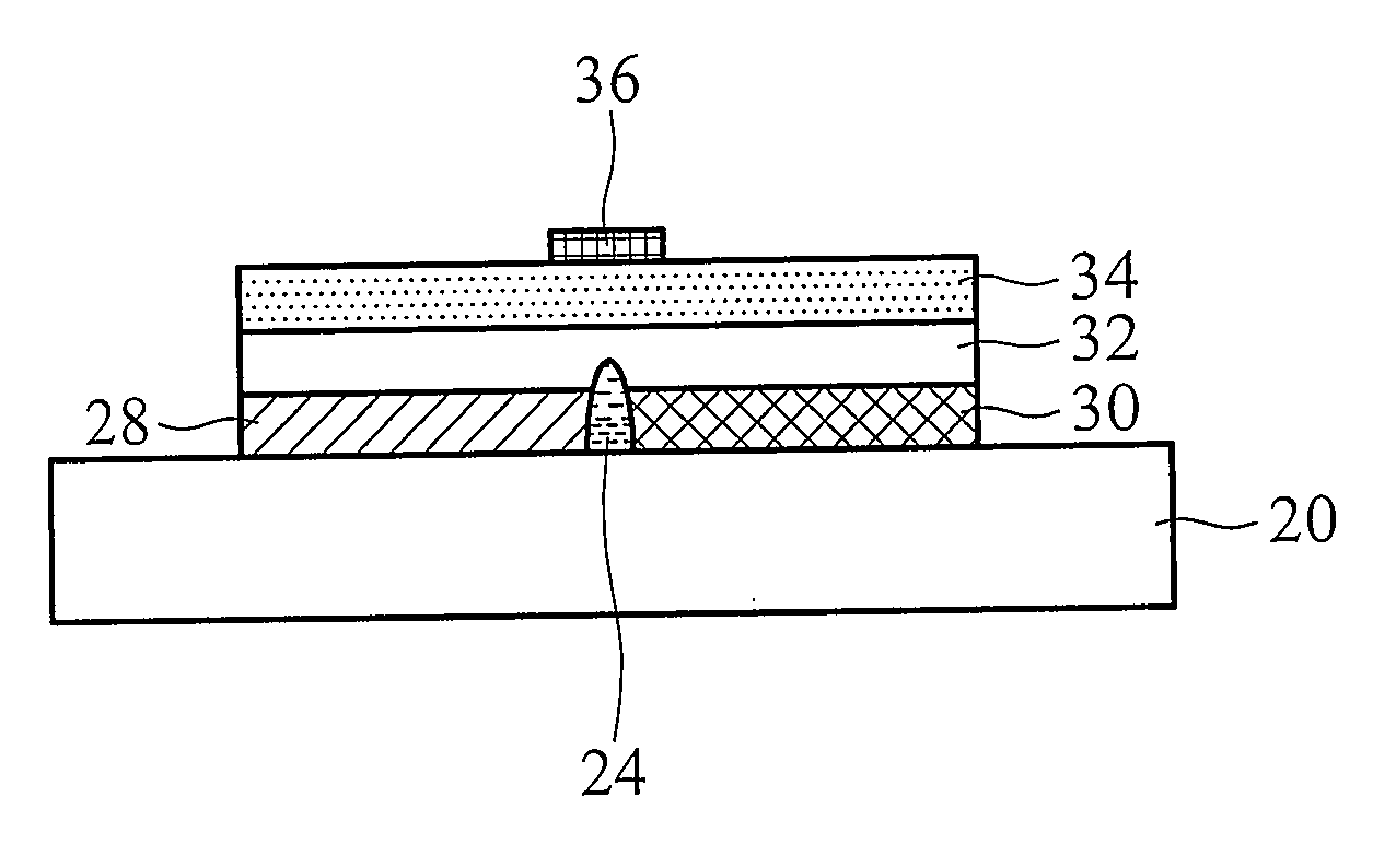
[0039]In one embodiment, the material of separating layer 46 may be the same as that of the third embodiment, wherein a solution of insulating material, such as PMMA, PVA or photoacrylate is dissolved in a solvent to form a solution for inkjet printing. The solvent may be a watery or oily liquid such as xylene. In the described bottom gate TFT, the separating layer is also a layer of graded concentration.

[0040]According to the invention, a micro-length of gate is formed by inkjet printing in combination with the coffee ring effect, and this has no need to be formed by photolithography. Use the micro-length of gate to achieve a reduced channel length of a TFT can get a high-current of the TFT.

[0041]Embodiments of the invention provide the following advantages. The micro-line of the coffee ring formed by inkjet printing can serve as a channel, source / drain, or gate of a TFT, wherein the micro-line can be formed of insulating, semiconductor, or conductive materials. TFTs with a circula...


PUM

PropertyMeasurementUnit
widthaaaaaaaaaa
widthaaaaaaaaaa
widthaaaaaaaaaa

Abstract

A thin-film transistor and method for fabricating a thin-film transistor is disclosed. In the method, a controlled micro-line is formed by inkjet printing in combination with the coffee ring effect. The micro-line may be a semiconductor or an insulator. A high-current thin-film transistor utilizing the micro-line of the coffee ring as a channel is formed. A high current TFT can be achieved by utilizing the micro-line structure of the coffee ring ridge as a TFT channel.

Description

BACKGROUND OF THE INVENTION[0001]1. Field of the Invention[0002]The invention relates to a thin-film transistor, and more particularly to a thin-film transistor formed by inkjet printing in combination with the coffee ring effect.[0003]2. Description of the Related Art[0004]Recently, organic material has been put to use in electronic device fabrication. A variety of photoelectric devices can be formed from combinations of organic electronic materials. Examples of photoelectric devices comprising organic electronic material included resistors, passive element capacitors, thin-film transistors, active element memory, displays, monitors, solar batteries, and others.[0005]Small electronic devices require small elements to achieve high resolution. Thin-film transistors (TFT) used in inorganic semiconductors among others, have been reduced to the 60 nm scale. Although 60 nm scale technology is applicable to general displays and electronic devices, organic material and soluble semiconducto...

Claims


Application Information

Patent Timeline
Patent Type & Authority Applications(United States)
IPC IPC(8): H01L29/786H01L21/336
CPCH01L51/0036H01L51/0037H01L51/102H01L51/0541H01L51/052H10K85/113H10K85/1135H10K10/471H10K10/464H10K10/82
Inventor LU, JHIH-PINGLEE, YUH-ZHENGHU, JE-PINGTSAI, HSUAN MINGCHENG, CHAO-KAI
Owner IND TECH RES INST
Why Eureka
Try Eureka