BGA package with leads on chip field of the invention

a technology of lead bundles and chips, applied in the field of bga package with lead bundles on the chip, can solve the problems of low reliability against moisture, falling of solder balls, and high cost of printed circuit boards, and achieve the effect of enhancing stability and reliability of wire bonding and solder ball placemen

Inactive Publication Date: 2008-02-21
CHIPMOS TECH INC
View PDF5 Cites 5 Cited by
  • Summary
  • Abstract
  • Description
  • Claims
  • Application Information

AI Technical Summary

Benefits of technology

[0021]Therefore, the leadless lead frame is used as a chip carrier in the BGA package 200 to resolve the solderability of solder balls and to enhance the stability and the reliability of wire bonding and solder ball placing. Moreover, the chip 220 with both central and peripheral bonding pads can be assembled with a leadless lead frame to become a BGA package.
[0022]In the second embodiment of the present invention, another BGA package is revealed. As shown in FIG. 4, the package 300 includes a leadless lead frame, a chip 320, a die-attaching layer 330, a plurality of bonding wires 340, an encapsulant 350, and a plurality of solder balls 360. The major components are about the same as the first embodiment. The leadless lead frame has a plurality of leads 310 where each lead 310 has a top surface 311 and a bottom surface 312. A wire bonding region 313 and a ball placing region 314 are defined on each bottom surface 312. The chip 320 has an active surface 321 and a back surface 322 where a plurality of first bonding pads 323 and at least a second bonding pad 324 are formed at the center and the periphery of the active surface 321 respectively. The die-att...

Problems solved by technology

However, the cost of the printed circuit board is much higher than the one of a lead frame and the reliability against moisture is also low.
However, the solder balls are totally exposed outside the package without any protection which leads to the ...

Method used


Image

  • BGA package with leads on chip field of the invention
  • BGA package with leads on chip field of the invention
  • BGA package with leads on chip field of the invention

Examples


Embodiment Construction

[0014]Please refer to the attached drawings, the present invention will be described by means of embodiment(s) below.

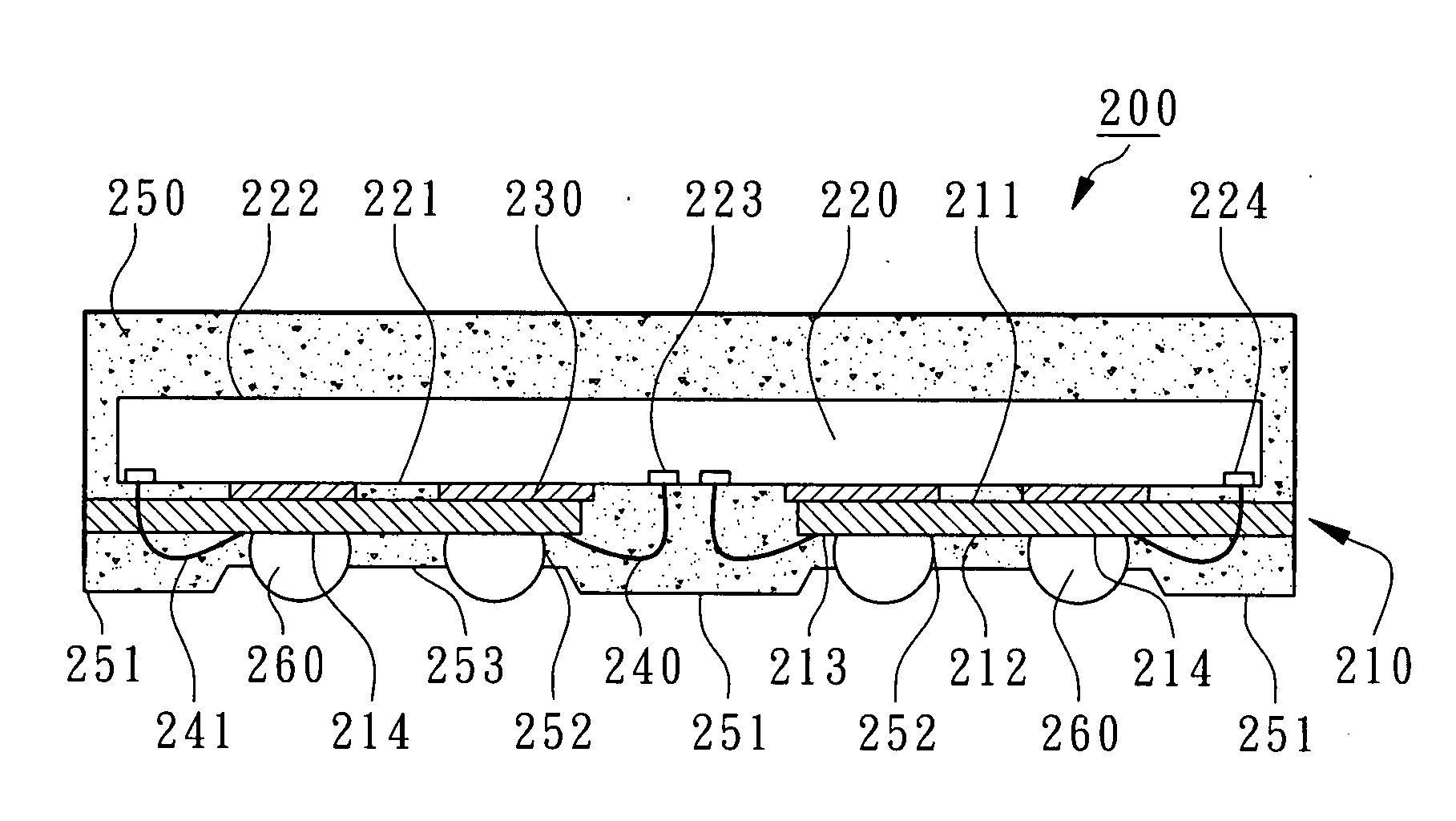
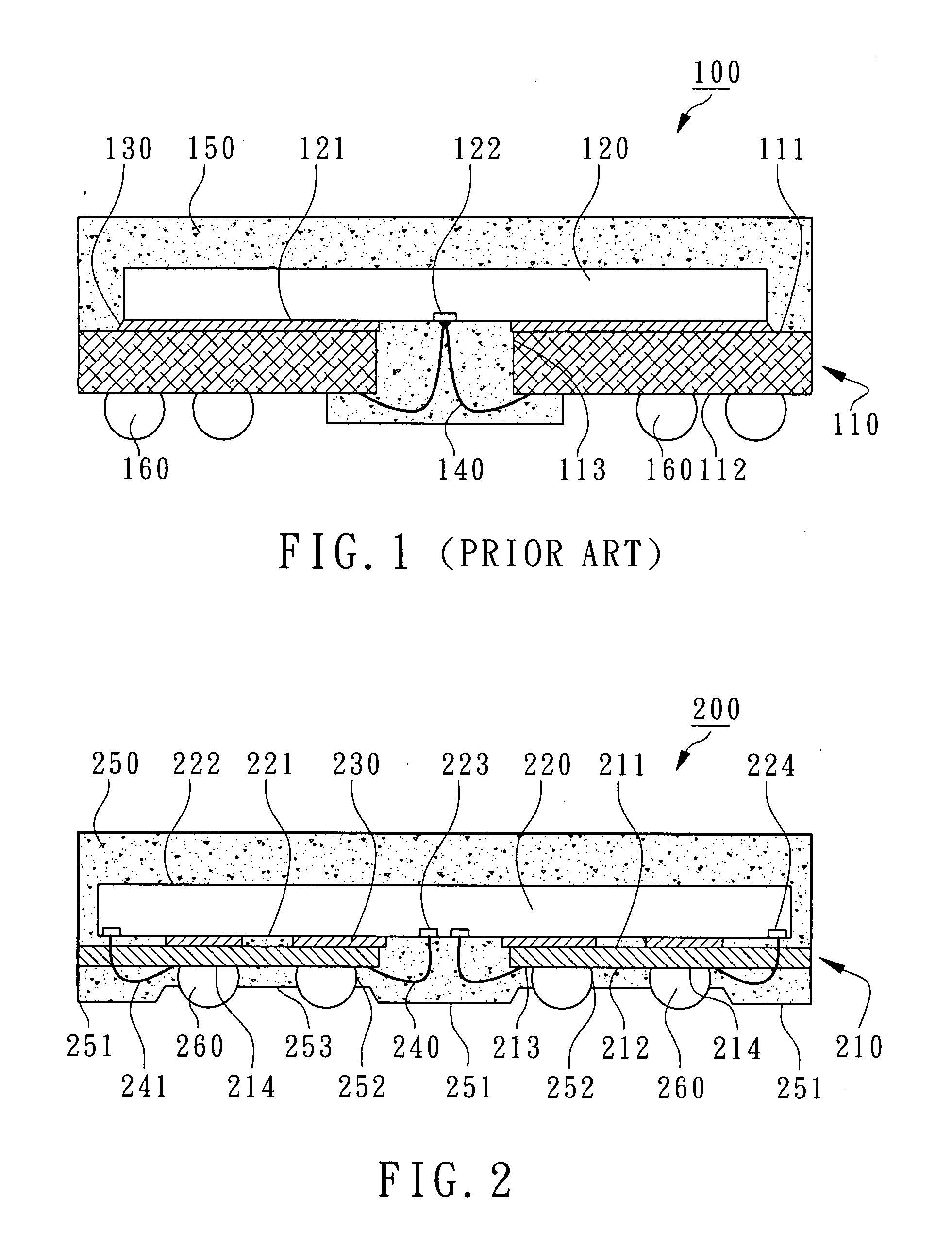
[0015]A BGA package with leads on a chip is disclosed according to the first embodiment. As shown in FIG. 2, a BGA package 200 primarily includes a leadless lead frame having a plurality of leads 210, a chip 220, a die-attaching layer 230, a plurality of bonding wires 240 and 241, an encapsulant 250, and a plurality of solder balls 260. The plurality of leads 210 have external ends aligned to the edges of the encapsulant 250. Normally, the materials of the leads 210 are metals such as copper, iron, or its alloys and are formed by punching or etching. Each lead 210 has a top surface 211 and a bottom surface 212 where each bottom surface 212 includes a wire bonding region 213 and a ball placing region 214 defined for bonding the bonding wires 240 and for placing the solder balls 260 respectively.

[0016]The chip 220 has an active surface 221 and a corresponding back surfa...


PUM


Abstract

A BGA package primarily includes a plurality of leads from a leadless lead frame, a chip, and a die-attaching layer. The chip is electrically connected to the leads by a plurality of bonding wires. Solder balls are disposed at the ball placing regions of the leads. Encapsulant encapsulates the chip, the die-attaching layer, and the top surfaces, the bottom surfaces, and the sides of the leads so that the ball placing regions are embedded inside the encapsulant. A plurality of cavities are formed in the encapsulant to expose the corresponding ball placing regions to resolve the solderability of the solder balls and to enhance the stability and reliability of wire bonding and solder ball placing. In one embodiment, a die-attaching layer between the chip and the leads is patterned for elastically supporting the solder balls and for wire bonding.

Description

FIELD OF THE INVENTION[0001]The present invention relates to a BGA (Ball Grid Array) package without printed circuit boards, and more particularly, to a BGA package with leads on a chip.BACKGROUND OF THE INVENTION[0002]The conventional Ball Grid Array packages (BGA) are always using printed circuit boards as chip carriers. In one kind of BGA packages, the active surfaces of chips face the printed circuit boards, and the bonding wires pass through the slots of the printed circuit boards. This kind of BGA package is often called Window BGA, Chip-On-Board BGA, or Chip-On-Substrate BGA.[0003]As shown in FIG. 1, a conventional BGA package 100 includes a printed circuit board 110, a chip 120, a die-attaching layer 130, a plurality of bonding wires 140, an encapsulant 150, and a plurality of solder balls 160. The printed circuit board 110 is made of BT (Bismaleimide Triazine resin) which has a top surface 111, a bottom surface 112, a slot 113 penetrating the top surface 111 and the bottom ...

Claims


Application Information

Patent Timeline
IPC IPC(8): H01L23/48
CPCH01L23/3114H01L23/4951H01L2924/00014H01L2224/06136H01L2224/06135H01L2924/181H01L2224/32225H01L24/48H01L2224/4824H01L2224/83194H01L2224/83856H01L2924/14H01L2924/1433H01L2924/15311H01L2924/00012H01L2224/45099H01L2224/45015H01L2924/207
Inventor LIN, HUNG-TSUN
Owner CHIPMOS TECH INC
Why Eureka
Try Eureka