Level converter and semiconductor device

a level converter and semiconductor technology, applied in logic circuits, pulse automatic control, pulse techniques, etc., can solve the problems of poor frequency of signal that can be communicated with a circuit the inability to communicate signals with high frequency using the abovementioned pmos-cml amplifier, so as to improve the characteristic of transistor deterioration, the effect of improving the frequency characteristics

Inactive Publication Date: 2008-02-21
RENESAS ELECTRONICS CORP
View PDF4 Cites 5 Cited by
  • Summary
  • Abstract
  • Description
  • Claims
  • Application Information

AI Technical Summary

Benefits of technology

[0013]According to the level converter of the present invention, the first and the third transistors operate as current sources for the source followers. Furthermore, an amplitude of an output signal is configured according to a ratio between resistances generated in the first and fourth transistors. That is, it is possible to reduce the resistance values of transistors while maintaining the resistance ratio between the first and fourth transistor and a resistance ratio between the second and the third transistor to be constant. Thus, frequency characteristic can be improved by increasing the amount of current supplied to the second and the fourth transistors operating as amplifier stages for the source followers so as to increase the carrier mobility of the transistors. Moreover, the amplitude of the output signal can be increased.
[0017]According to the level converter and semiconductor device of the present invention, the deterioration of frequency characteristics by the characteristic of the transistor can be improved.

Problems solved by technology

However, it is generally known that as PMOS transistors have carrier mobility lower than NMOS transistors, a frequency of signal that can be communicated is poorer than NMOS transistors.
Therefore, we have now discovered that to process a CML level signal having a low signal level, there is a problem that a signal with high frequency cannot be communicated by a circuit using the abovementioned PMOS-CML amplifier.

Method used


Image

  • Level converter and semiconductor device
  • Level converter and semiconductor device
  • Level converter and semiconductor device

Examples


first embodiment

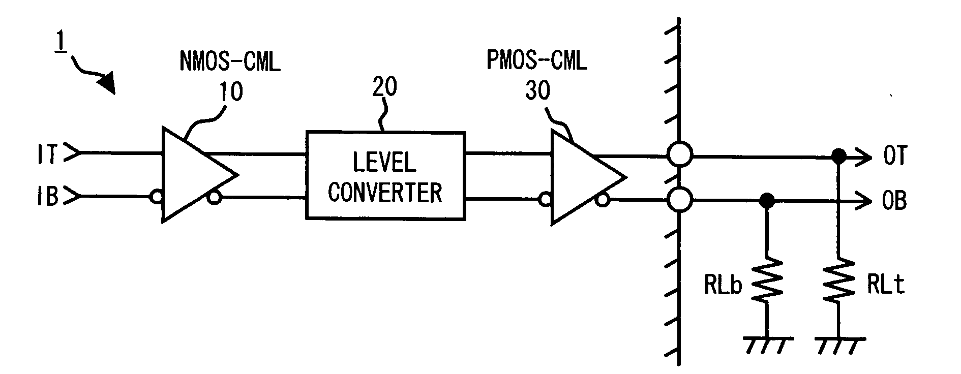
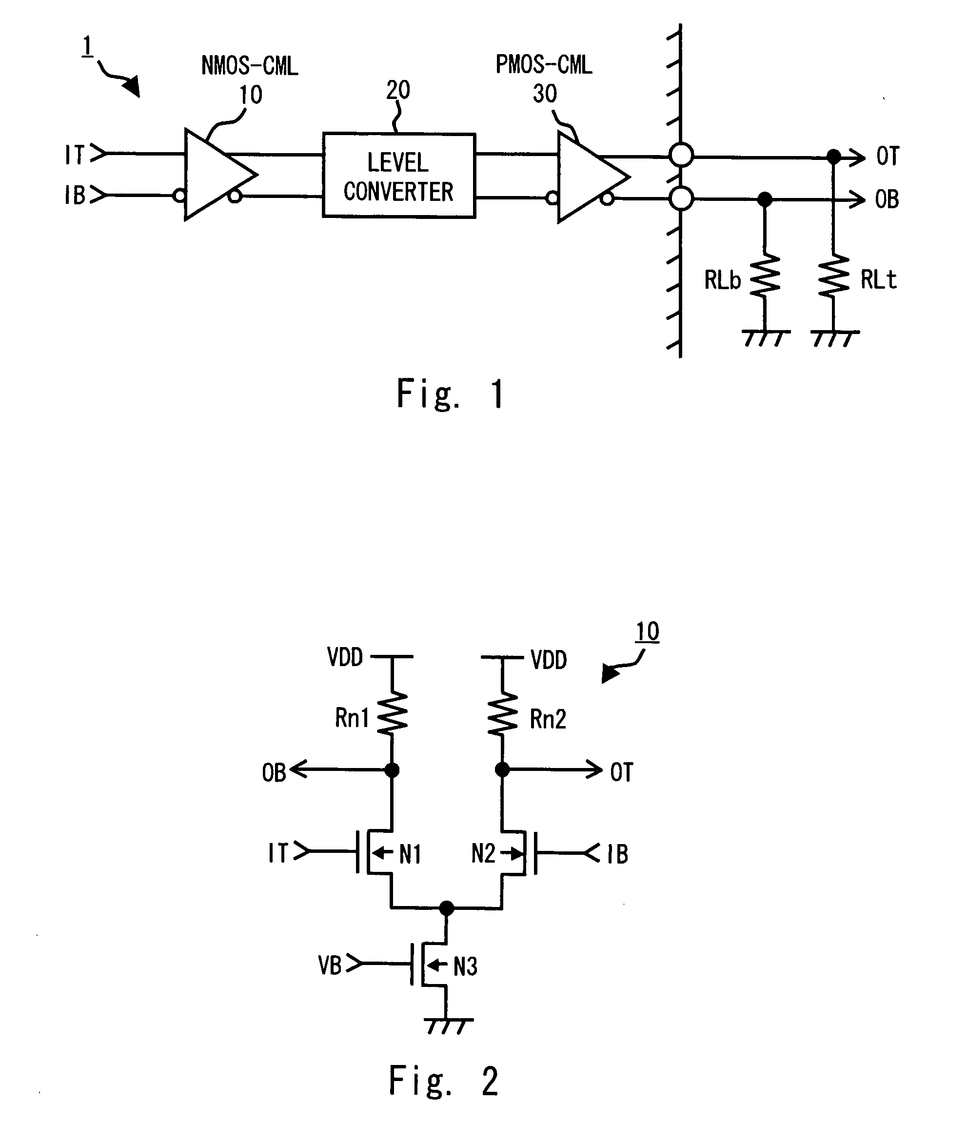
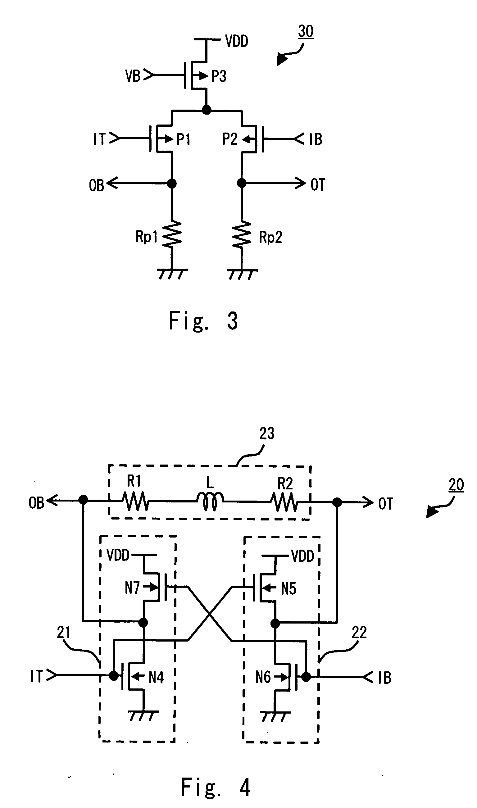
[0035]In a first embodiment, a case is described in which a circuit of the present invention is used for a transmitting circuit of a semiconductor device. A block diagram of a transmitting circuit 1 according to a first embodiment is illustrated in FIG. 1. As shown in FIG. 1, the transmitting circuit 1 includes a NMOS-CML amplifier 10, level converter 20 and PMOS-CML amplifier 30. In the first embodiment, the NMOS-CML amplifier 10 is used as a first level converter, PMOS-CML amplifier 30 is used as a second level converter and the level converter 20 is used as a third level converter. Note that a semiconductor device has circuits (not shown) for processing other signal processes in addition to the transmitting circuit 1. Furthermore, differential signals (IT and IB in FIG. 1) input to the NMOS-CML amplifier 10 are generated by those circuits.

[0036]The NMOS-CML amplifier 10 converts a signal level of the differential input signals IT and IB into a first signal level (for example NMOS...

second embodiment

[0063]A semiconductor device of a second embodiment forms a receiving circuit 2 using the NMOS-CML amplifier 10 and PMOS-CML amplifier 30 of the first embodiment. In the second embodiment, a level converter 40 for converting a PMOS-CML level signal into a NMOS-CML level signal is included.

[0064]FIG. 10 is a block diagram of the receiving circuit 2. The receiving circuit 2 according to the second embodiment is described hereinafter in detail with reference to FIG. 10. The receiving circuit 2 is a receiving unit for a signal input to the semiconductor device. As shown in FIG. 10, the receiving circuit 2 includes the NMOS-CML amplifier 10, the level converter 40 and the PMOS-CML amplifier 30. In the second embodiment, the PMOS-CML amplifier 30 is used as a first level converter, the NMOS-CML amplifier 10 is used as a second level converter and the level converter 40 is used as a third level converter. Note that in addition to the receiving circuit 2, the semiconductor device includes a...


PUM


Abstract

A level converter includes a first to fourth transistors formed of a semiconductor having a same conductivity type. The first transistor is connected between a first power supply and a second output terminal, the second transistor is connected between a second power supply and a first output terminal, the third transistor is connected between the first power supply and the first output terminal, the fourth transistor is connected between the second power supply and the second output terminal, the first and the second transistors are input with one of first differential signals and the third and the fourth transistors are input with another of the first differential signals.

Description

BACKGROUND OF THE INVENTION[0001]1. Field of the Invention[0002]The present invention relates to a level converter and a semiconductor device, and particularly to a level converter and a semiconductor device for suppressing an attenuation of a signal communicated across wide band.[0003]2. Description of Related Art[0004]In recent years, an operating speed of a semiconductor device is increasing. Thus a frequency of a signal transmitted and received between semiconductor devices is increasing. To transmit / receive such a high frequency signal, generally an amplitude of the signal is reduced and the signal is treated as a differential signal. By reducing the amplitude of the signal, it is possible to generate a signal that changes at high speed without increasing the current driving capability of output buffer. Furthermore, by treating the signal as a differential signal, it is possible to improve noise immunity of a small amplitude signal. For such a small amplitude signal, there is a...

Claims


Application Information

Patent Timeline
Patent Type & Authority Applications(United States)
IPC IPC(8): H03L5/00
CPCH03K19/018528G11C7/00
Inventor AOKI, YASUSHI
Owner RENESAS ELECTRONICS CORP
Why Eureka
Try Eureka