Calibration circuit

a circuit and calibration circuit technology, applied in the field of calibration circuits, can solve the problems of affecting the impedance of the output buffer, the calibration operation takes a certain amount of time to compare voltage and the change of the impedance of the replica buffer, and the calibration operation is not suitable for continuous operation. , to achieve the effect of sufficient calibration operation

Inactive Publication Date: 2008-02-21
LONGITUDE SEMICON S A R L
View PDF9 Cites 14 Cited by
  • Summary
  • Abstract
  • Description
  • Claims
  • Application Information

AI Technical Summary

Benefits of technology

[0022]According to the present invention, when a first calibration command is issued, not both a calibration operation for a first replica buffer and a calibration operation for a second replica buffer but either of them is performed. Accordingly, the number of updates of impedance in a calibration period is increased, and even if the frequency of an external clock is high, a sufficient calibration operation can be performed.

Problems solved by technology

If the input / output signals have reduced amplitudes, the desired accuracy of impedances of output buffers becomes severe.
Also, during its actual use, the impedance of the output buffer is affected by variations in ambient temperature and power source voltage.
However, the comparison of voltage and the change of impedance of the replica buffer in the calibration operation take a certain amount of time.
In such a case, the calibration operation cannot be performed.

Method used


Image

  • Calibration circuit
  • Calibration circuit
  • Calibration circuit

Examples


Embodiment Construction

[0037]Preferred embodiments of the present invention will now be explained in detail with reference to the drawings.

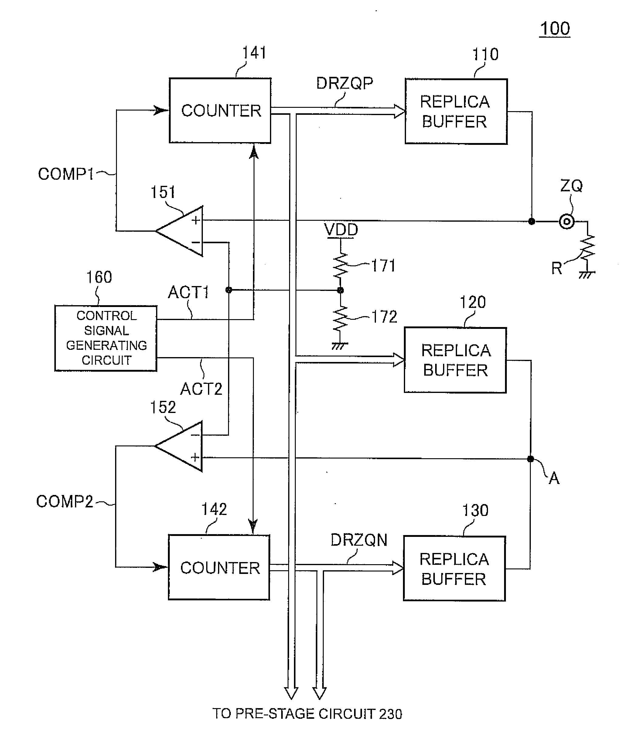
[0038]FIG. 1 is a circuit diagram of a calibration circuit 100 according to a preferred embodiment of the present invention.

[0039]As shown in FIG. 1, the calibration circuit 100 of the present embodiment includes replica buffers 110, 120, and 130, a counter 141 for controlling the impedances of the replica buffers 110 and 120, a counter 142 for controlling the impedance of the replica buffer 130, a comparator 151 for controlling the counter 141, a comparator 152 for controlling the counter 142, and a control signal generating circuit 160.

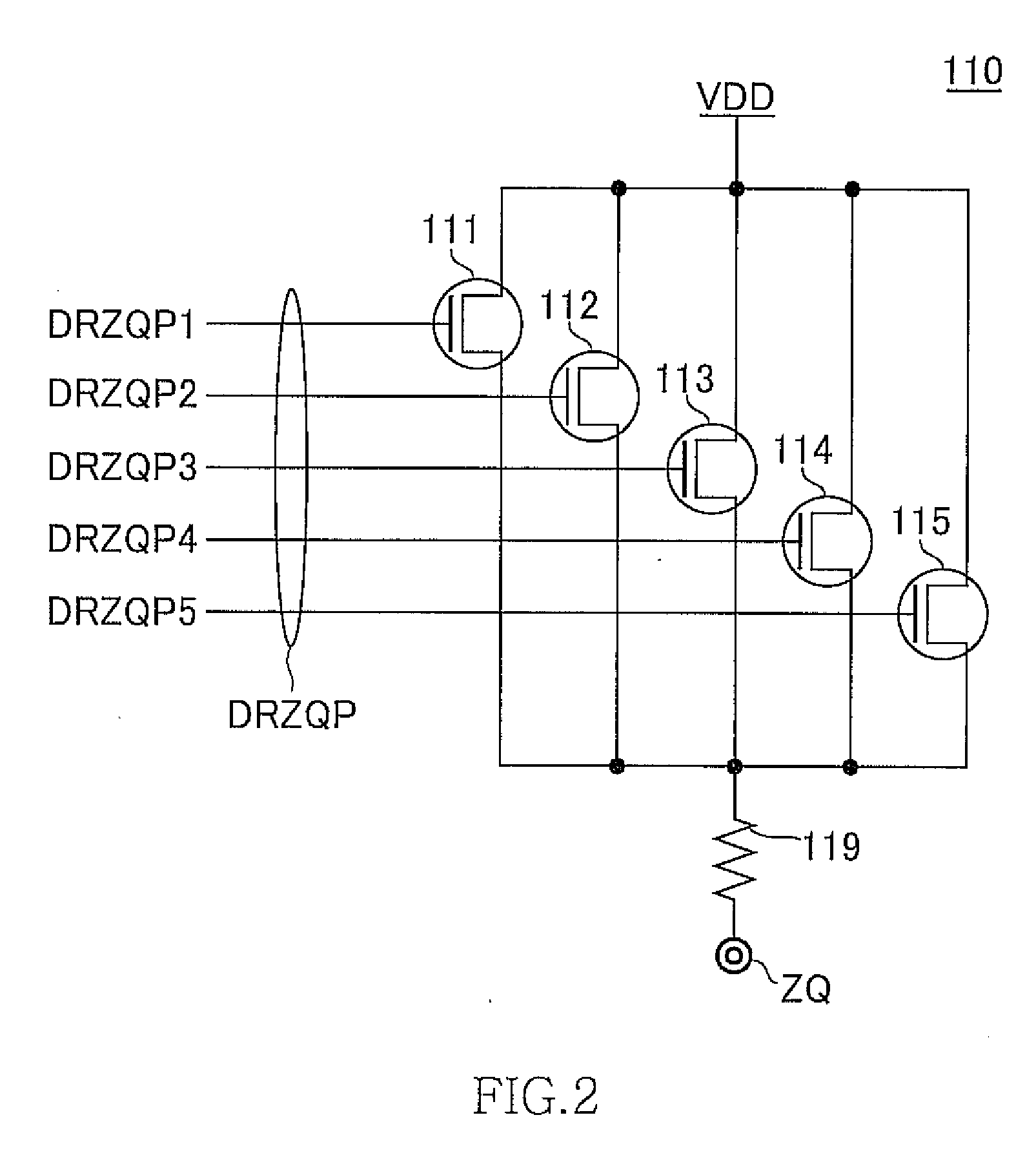
[0040]The replica buffers 110, 120, and 130 have the same circuit configuration as a part of an output buffer which will be described later. The output impedance is adjusted by using the replica buffers 110, 120, and 130 and the result is reflected in the output buffer. The impedance of the output buffer is thus set to the desired valu...


PUM


Abstract

To include a first replica buffer that has substantially the same circuit configuration as a pull-up circuit which constitutes an output buffer and a second replica buffer that has substantially the same circuit configuration as a pull-down circuit which constitutes the output buffer. When a first calibration command ZQCS is issued, either a control signal ACT1 or ACT2 is activated, and a calibration operation is performed for either the first replica buffer or the second replica buffer. When a second calibration command ZQCL is issued, both of the control signals ACT1, ACT2 are activated and the calibration operation is performed for both the first replica buffer and the second replica buffer.

Description

TECHNICAL FIELD[0001]The present invention relates to a calibration circuit, and, particularly to a calibration circuit for adjusting the impedance of an output buffer provided in a semiconductor device. The present invention also relates to a data processing system that includes a semiconductor memory device having a calibration circuit.BACKGROUND OF THE INVENTION[0002]In recent years, significantly high data transfer rate is required for data transfer between semiconductor devices (between CPUs and memories for example). To accomplish high data transfer rate, the amplitude of input / output signals is increasingly reduced. If the input / output signals have reduced amplitudes, the desired accuracy of impedances of output buffers becomes severe.[0003]The impedance of the output buffer varies depending on process conditions during the manufacturing. Also, during its actual use, the impedance of the output buffer is affected by variations in ambient temperature and power source voltage. ...

Claims


Application Information

Patent Timeline
Patent Type & Authority Applications(United States)
IPC IPC(8): G06F19/00G06F3/00G11C11/401G11C11/4093H03K19/0175H03K19/0948
CPCH03F1/56H03F2200/456H03F2200/453H03F2200/366
Inventor YOKO, HIDEYUKIFUJISAWA, HIROKI
Owner LONGITUDE SEMICON S A R L
Why Eureka
Try Eureka