Field effect transistor and image display apparatus using the same

a field effect transistor and image display technology, applied in the direction of optics, instruments, radioation control devices, etc., can solve the problems of difficult reduction of power consumption in low-voltage drives, difficult realization of image display apparatus of low power consumption,

Inactive Publication Date: 2002-08-29
PANASONIC LIQUID CRYSTAL DISPLAY CO LTD +1
View PDF0 Cites 23 Cited by
  • Summary
  • Abstract
  • Description
  • Claims
  • Application Information

AI Technical Summary

Benefits of technology

0027] It is therefore an object of the present invention to provide a field effect transistor that operates sufficiently at low voltages.

Problems solved by technology

This technique, however, fails to allow for TFTs that operate at low voltages, so that image display apparatus of low power consumption are difficult to realize because the conventional TFTs are difficult to drive at low voltages.
That is, the operational voltage of the TFT is so high that a reduction in the power consumption in the low-voltage drive is difficult.

Method used


Image

  • Field effect transistor and image display apparatus using the same
  • Field effect transistor and image display apparatus using the same
  • Field effect transistor and image display apparatus using the same

Examples


first embodiment

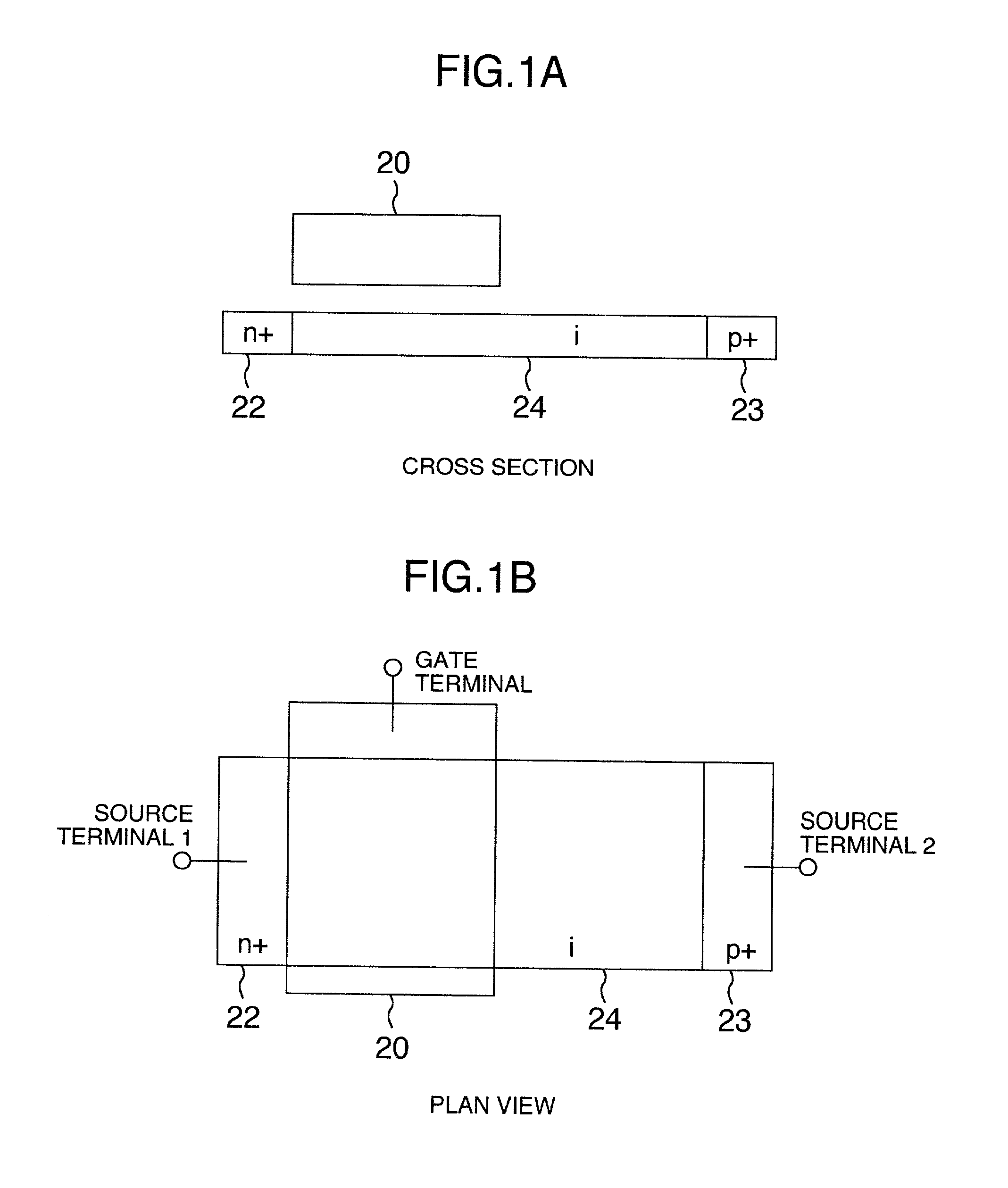
[0061] Referring to FIGS. 1-9, a first embodiment of the present invention will be described. As shown in FIG. 2, a polysilicon TFT liquid crystal display panel of this embodiment comprises a glass substrate 14 on which pixels 1 each having liquid crystal capacitance 4 are arranged in the form of a matrix (for convenience of simplification, only four pixels are illustrated).

[0062] The liquid crystal capacitance 4 of each pixel 1 is connected to an associated signal line 9 via two pixel TFTs 2 and 3 whose source and drain electrodes are connected in series and whose gate electrodes are connected together to an associated gate line 5.

[0063] The respective pixels 1 in a row are connected in parallel with the associated gate line 5, which is, in turn, connected via a corresponding gate line buffer 8 and a gate line level shifter 7 to a gate line shift register 6.

[0064] The respective pixels in a column are connected in parallel with the corresponding signal line 9, which is, in turn, co...

second embodiment

[0149] A second embodiment of the present invention will be described next. FIG. 10 illustrates a polycrystal silicon TFT liquid crystal display panel of the second embodiment. Also, in this embodiment a glass substrate 14 is provided on which pixels 1 each having crystal capacitance 4 are arranged in the form of a matrix as in the first embodiment of FIG. 2 (similarly, for simplifying purposes, only four pixels 1 are illustrated).

[0150] The liquid crystal capacitance 4 of the pixels 1 in each column are together connected to a respective signal line 9 via respective pairs of pixel TFTs 2 and 3 of the pixels where the source and drain electrodes of each TFT are connected in series. The respective pixels 1 in each row are connected in parallel to a respective gate line 5 through the gate electrodes of the pair of TFTs 2 and 3 thereof. Each gate line 5 is connected via a relevant gate line buffer 8 and a gate line level shifter 7 to gate line shift register 6.

[0151] Thus, this arrange...

third embodiment

[0177] A third embodiment of the present invention will be described next. The composition and operation of a polycrystal silicon TFT liquid crystal display panel according to this embodiment are substantially the same as in the first embodiment already described above. Thus, further description thereof will be omitted and the difference of the third embodiment from the first embodiment will be described below.

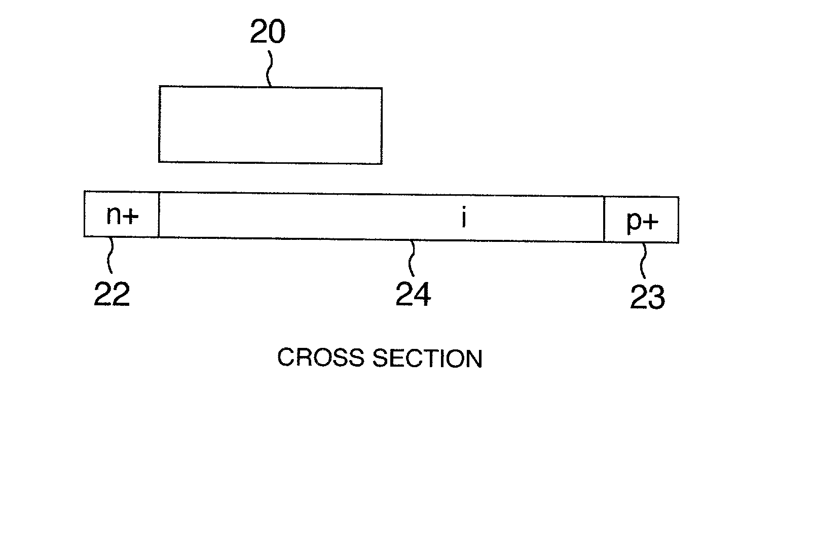
[0178] FIG. 13 illustrates a composition of a bipolar TFT used in the third embodiment and corresponds to the cross-sectional view of FIG. 1A described with reference to the first embodiment. As shown in FIG. 13, the bipolar TFT of the third embodiment has a first source area composed of an n.sup.+ high-density impurity injection area 122 (corresponding to 22 in FIG. 1A), a second source area composed of a p.sup.+ high-density impurity injection area 123 (corresponding to 23 in FIG. 1A), a channel forming area composed of an i-impurity non-injection area 124 (corresponding to ...


PUM

PropertyMeasurementUnit
gate voltageaaaaaaaaaa
drive voltageaaaaaaaaaa

Abstract

A field effect transistor includes an n+ high-density impurity injection area, a p+ high-density impurity injection area, an i-impurity non-injection area, and a gate electrode. The gate electrode is free from completely lapping over the i-impurity non-injection area, but laps over substantially half the i-impurity non-injection area adjacent to the n+ high-density impurity injection area so as to avoid channel carrier capture levels due to crystal defects/grain boundaries and an effect of potential barriers due to the channel carrier capture levels.

Description

[0001] 1. Field of the Invention[0002] The present invention relates to field effect transistors and image display apparatus using the same, and more particularly to a field effect transistor operable at low voltages and image display apparatus capable of displaying an image at low power consumption.[0003] 2. Description of the Related Art[0004] Recently, the advancement of liquid crystal display apparatus has been remarkable and thin display apparatus have rapidly diffused in place of CRTs (Cathode Ray Tubes) as the display devices that have been prevalent so far. As personal computers (PCs), digital video discs (DVDs), and digital television broadcasts have diffused, the thin display apparatus have been required to present a high-speed response and high-definition display. TFT liquid crystal display panels have been known as liquid crystal display devices capable of meeting such requirement in the past.[0005] Referring to FIG. 19, one example of the conventional TFT liquid crystal...

Claims


Application Information

Patent Timeline
Patent Type & Authority Applications(United States)
IPC IPC(8): G02F1/1368H01L21/336H01L21/8234H01L27/08H01L27/088H01L27/146H01L29/739H01L29/786
CPCH01L27/14679H01L29/7391Y10S257/912
Inventor AKIMOTO, HAJIME
Owner PANASONIC LIQUID CRYSTAL DISPLAY CO LTD
Why Eureka
Try Eureka