Image sensor module

a technology of image sensor and module, which is applied in the field of image sensor module, can solve the problems of inability to meet the current requirements of electronic products, low working efficiency or short life time, and achieve the effect of reducing the height reducing the internal temperature of the chip, and reducing the internal temperature of the image sensor modul

Active Publication Date: 2008-02-28
ADVANCED SEMICON ENG INC
View PDF6 Cites 17 Cited by
  • Summary
  • Abstract
  • Description
  • Claims
  • Application Information

AI Technical Summary

Benefits of technology

[0011]The present invention can solve the internal heat dissipation problem for the image sensor module.
[0013]Furthermore, the present invention provides an image sensor module, wherein the electrical connection between an image signal processor and a substrate of the image sensor module is well maintained.
[0015]In the present invention, the image signal processor is disposed in the concave of the substrate, to reduce the height of the image sensor module. In addition, the image sensor chip can be disposed on a heat sink so as to reduce the internal temperature of the chip. Further, the concave of the substrate may have at least one vent hole at the bottom, so that the heat within the image sensor module can be dissipated to the ambient environment via the vent holes due to the convection effect. Therefore, the internal temperature of the image sensor module can be reduced.

Problems solved by technology

However, the conventional image signal processor 120 is disposed on the bottom surface 110a of the substrate 110 in the form of a module, such that the whole image sensor module 100 has a larger thickness, which thus cannot satisfy the current requirements for the electronic products of being light, slim, short, small and portable.
However, in the image sensor module 200, overheat of the image sensor chip 230 and the image signal processor 220 may easily occurs and lead to low working efficiency or short life time due to the stacked disposition between the image sensor chip 230 and the image signal processor 220.

Method used


Image

  • Image sensor module
  • Image sensor module
  • Image sensor module

Examples


Embodiment Construction

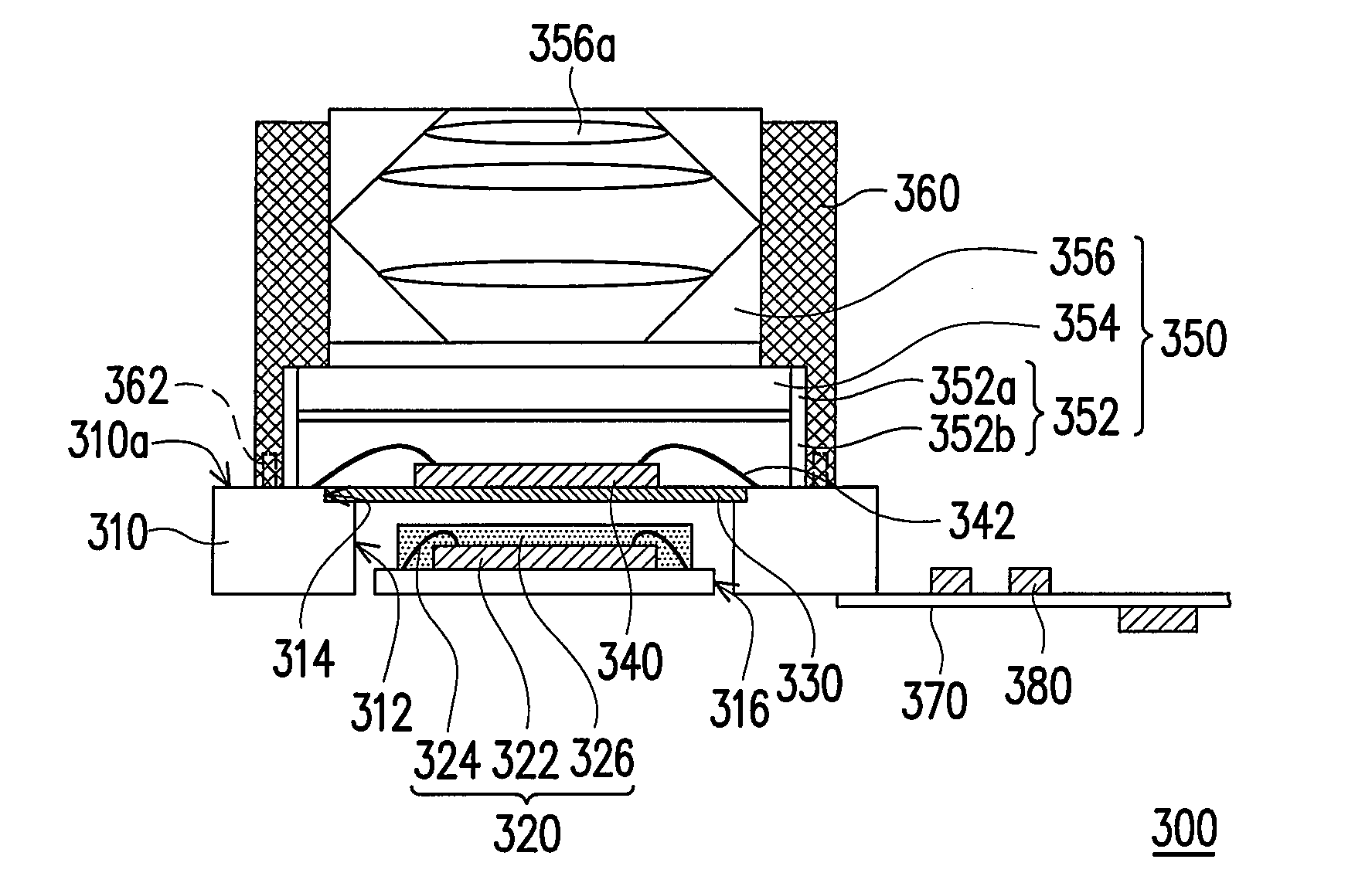
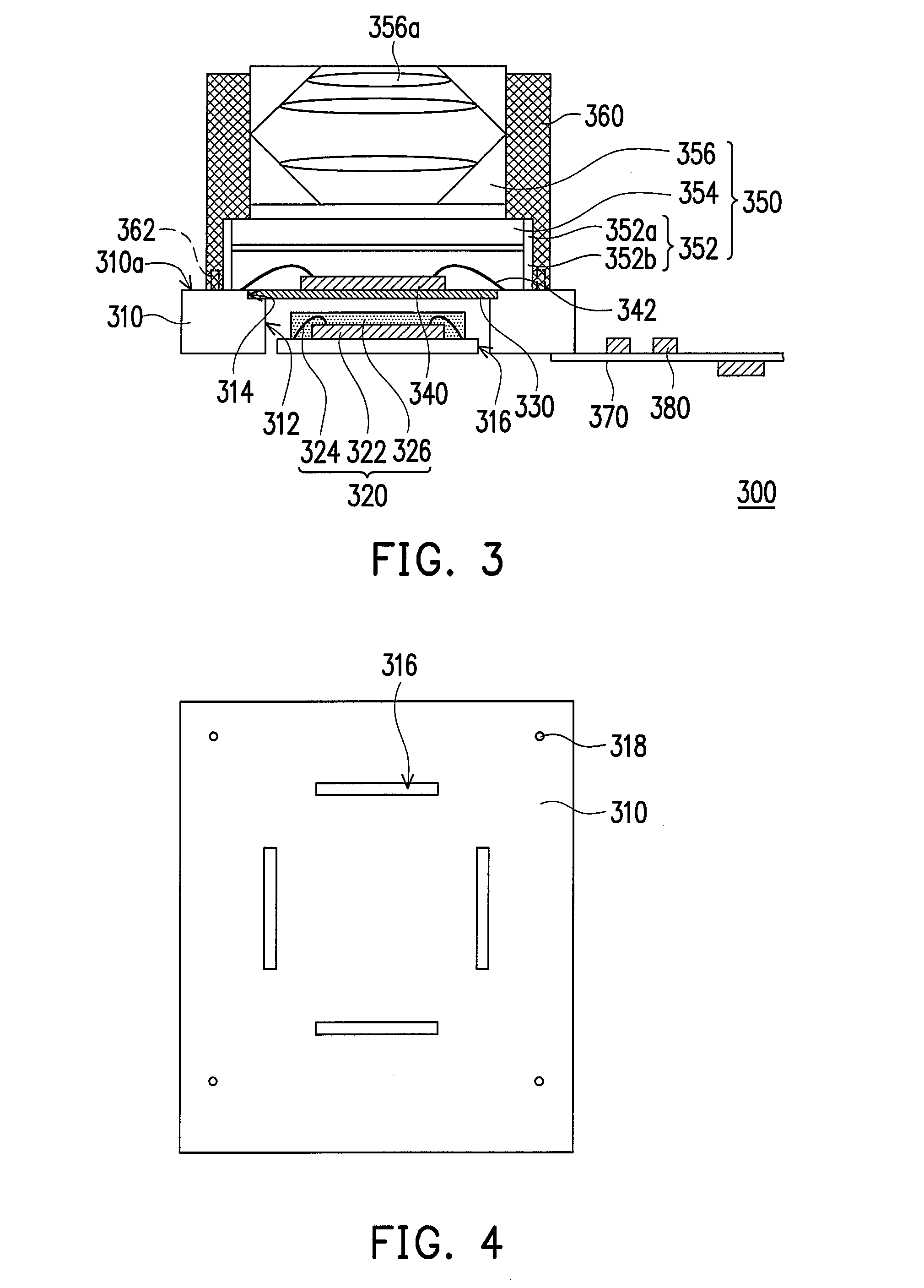
[0023]FIG. 3 is a schematic view of an image sensor module according to a preferred embodiment of the present invention. Referring to FIG. 3, the image sensor module 300 comprises a substrate 310, an image signal processor 320, a supporting board 330, an image sensor chip 340 and a cover 350. A concave 312 is located on a surface 310a of the substrate 310. The image signal processor 320 is disposed in the concave 312 of the substrate 310, and is electrically connected to the substrate 310, wherein the depth of the concave 312 is greater than the thickness of the image signal processor 320. In an embodiment of the present invention, the image signal processor 320 comprises an image signal processing chip 322, a plurality of wire-bonding wires 324 and a molding compound 326. The image signal processing chip 322 is electrically connected to the substrate 310 via the wire-bonding wires 324. The molding compound 326 covers the image signal processing chip 322 and the wire-bonding wires 3...


PUM


Abstract

An image sensor module including a substrate, an image signal processor, a supporting board, an image sensor chip and a cover is provided. A concave is located on a surface of the substrate. The image signal processor is disposed in the concave, and is electrically connected to the substrate. The supporting board is disposed on the surface of the substrate and covers the concave. The image sensor chip is disposed on the supporting board and electrically connected to the substrate. The cover is disposed on the substrate, and covers the image sensor chip.

Description

CROSS-REFERENCE TO RELATED APPLICATION[0001]This application claims the priority benefit of Taiwan application serial no. 95131531, filed Aug. 28, 2006. All disclosure of the Taiwan application is incorporated herein by reference.BACKGROUND OF THE INVENTION[0002]1. Field of the Invention[0003]The present invention relates to a sensor module, and more particularly, to an image sensor module.[0004]2. Description of Related Art[0005]The process for manufacturing CMOS image sensor (CIS) is compatible with that for manufacturing CMOS transistor. As this image sensor can be easily integrated with other peripheral circuits onto the same chip, the cost and power consumption of the image sensor are greatly reduced. In recent years, the CMOS image sensor has replaced the charge-coupled device (CCD) in the lower level application and has become popular day by day.[0006]FIG. 1 is a schematic view of a conventional image sensor module. The conventional image sensor module 100 comprises a substra...

Claims


Application Information

Patent Timeline
Patent Type & Authority Applications(United States)
IPC IPC(8): H01L27/00
CPCH01L27/14618H04N5/2257H04N5/2254H04N5/2253H01L2224/32145H01L2224/48091H01L2224/73265H01L2924/00014
Inventor CHEN, JIAN-CHENGCHENG, MING-HSIANGLEE, CHIA-JUNG
Owner ADVANCED SEMICON ENG INC
Why Eureka
Try Eureka