Monolithically integratable circuit arrangement

a circuit arrangement and monolithic technology, applied in the direction of impedence networks, multiple-port networks, inductances, etc., can solve the problems of increasing parasitic effects, affecting the efficiency of vco circuits, and affecting the arrangement of elements in the area of both ends of conductor loops, so as to achieve simple and cost-effective implementation, facilitate symmetric operation, and reduce space requirements

Inactive Publication Date: 2008-02-28
ATMEL CORP
View PDF19 Cites 27 Cited by
  • Summary
  • Abstract
  • Description
  • Claims
  • Application Information

AI Technical Summary

Benefits of technology

[0011]It is therefore an object of the present invention to provide a circuit arrangement, which is simple and cost-effective to implement, has a reduced space requirement, enables symmetric operation, and can be used flexibly in oscillators, mixers, amplifiers, filters, matching circuits, etc., without detrimentally affecting their efficiency.

Problems solved by technology

It is a disadvantage here that the arrangement of the elements in the area of both ends of the conductor loop is problematic.
The capacitive elements Ct, Cd require a relatively large (chip) area, so that long supply lines are needed in part, which causes an increase in parasitic effects, or else the surface area of the capacitive elements must be limited, which has a disadvantageous effect on the efficiency of the VCO circuit (limited frequency tunability, rather high phase noise, etc.).
Another disadvantage is that even minor differences in the resistance values of the two bias resistors Rb, e.g., due to technology or process variations, lead to different potentials at the bases of the transistors and thereby to different collector currents.
This has the result of an asymmetric operation (offset), which disadvantageously results in increased noise and a lower output power.
It is disadvantageous in addition that the blocking capacitors Cd narrow the usable frequency tuning range and as a result of parasitic capacitors worsen the entire electrical behavior of the circuit.

Method used


Image

  • Monolithically integratable circuit arrangement
  • Monolithically integratable circuit arrangement
  • Monolithically integratable circuit arrangement

Examples


Embodiment Construction

[0037]In the figures, the same and functionally identical elements and signals, if not specified otherwise, are provided with the same reference characters.

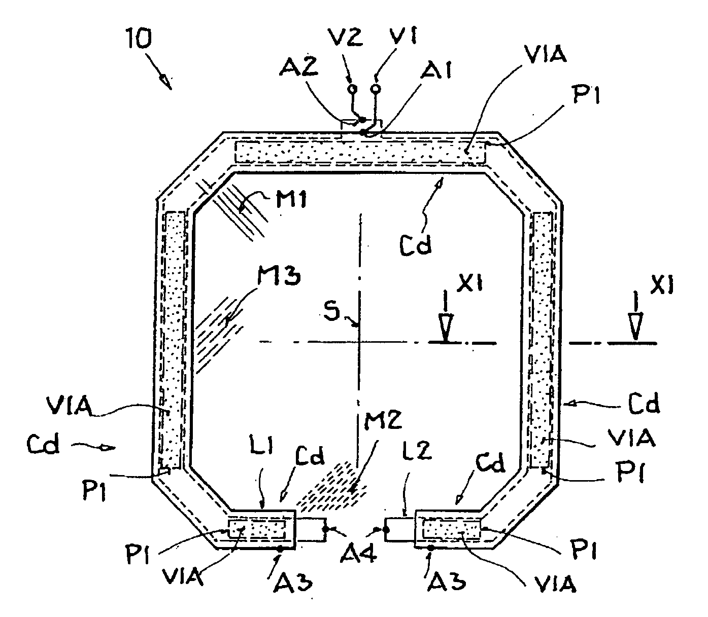
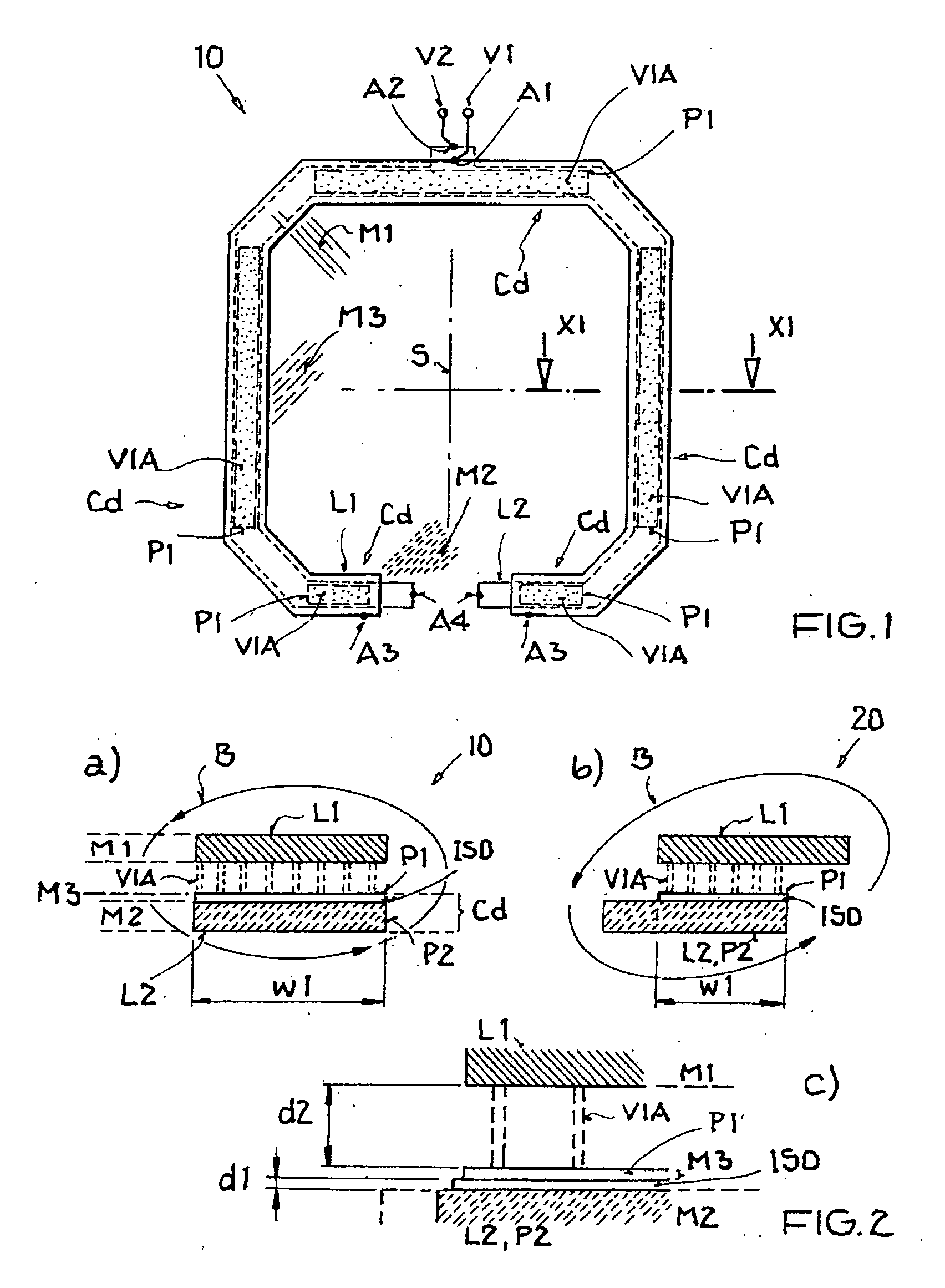
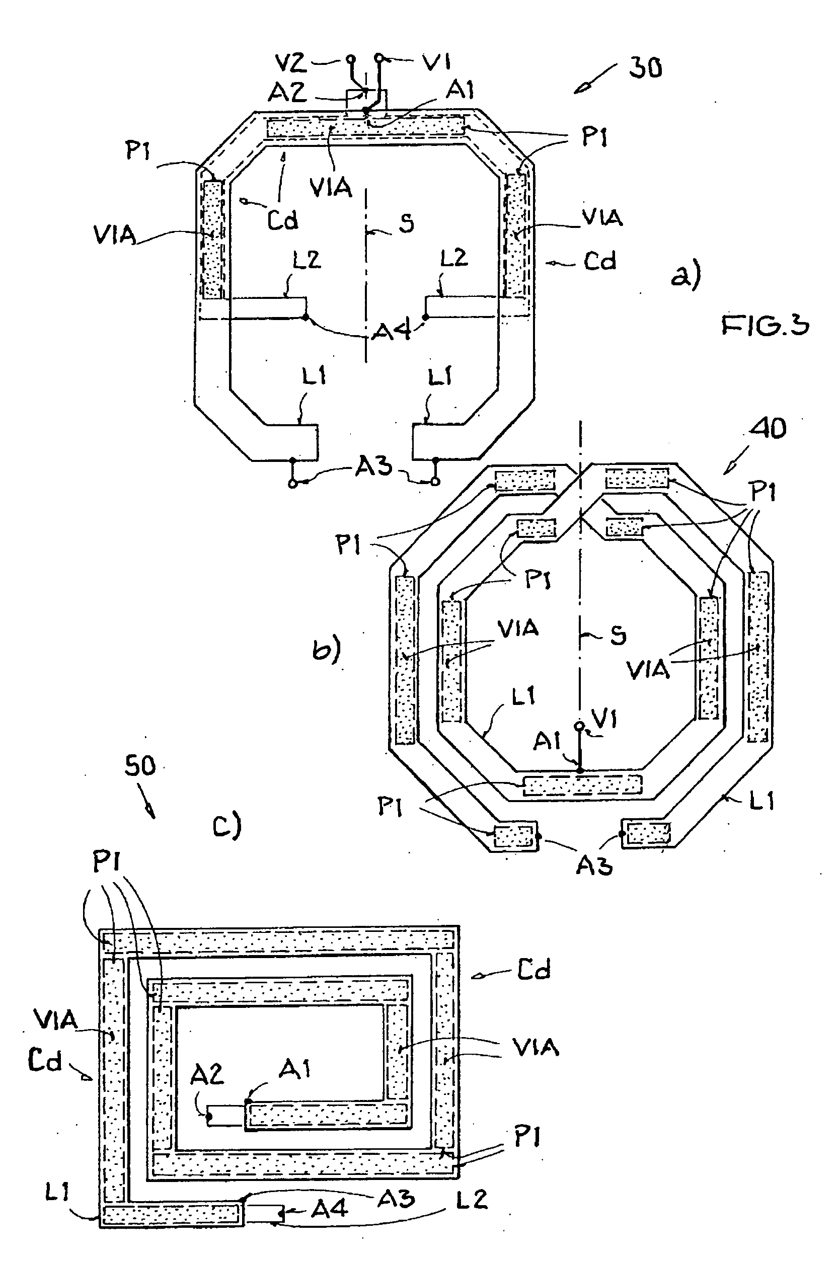
[0038]FIG. 1 shows a layout of a first exemplary embodiment of a circuit arrangement of the invention in a plan view.

[0039]The monolithically integrated circuit arrangement 10 has a conductor loop L1 placed in a first (upper) metallization level M1 and a conductor loop L2 placed in a second (lower) metallization level M2. Conductor loop L1 is equipped with a DC terminal A1 to apply a first DC potential V1 and with an AC terminal A3 to apply or tap off a first high-frequency signal, whereas conductor loop L2 has a DC terminal A2 to apply a second DC potential V2 and an AC terminal A4 to apply or tap off a second high-frequency signal.

[0040]Furthermore, a plurality of integrated metal-isolator-metal (MIM) capacitors Cd is provided with one each of a first (upper) capacitor plate P1 depicted as a rectangle, which are placed in a thi...


PUM


Abstract

A monolithically integratable circuit arrangement is provided, which has at least one inductor, formed as a conductor loop, and at least one capacitor, connected to the conductor loop. According to the invention, the circuit arrangement comprises (a) at least one first conductor loop placed in at least one first metallization level and having a first DC terminal for applying a first DC potential, (b) at least one second conductor loop placed in at least one second metallization level and having a second DC terminal for applying a second DC potential, (c) at least one metal-isolator-metal capacitor with a capacitor plate, which is placed in a third metallization level between the first and second metallization level, and (d) at least one metallic connecting means placed between the capacitor plate and the first conductor loop, said means which connects the capacitor plate in an electrically conducting manner to the first conductor loop. The invention relates furthermore to an integrated circuit having a circuit arrangement of this type.

Description

[0001]This nonprovisional application claims priority to German Patent Application No. DE 10 2006 035 204, which was filed in Germany on Jul. 29, 2006, and to U.S. Provisional Application No. 60 / 834,171, which was filed on Jul. 31, 2006, and which are both herein incorporated by reference.BACKGROUND OF THE INVENTION[0002]1. Field of the Invention[0003]The present invention relates to a monolithically integratable circuit arrangement having at least one inductor, formed as a conductor loop, and at least one capacitor, connected to the conductor loop, and relates to an integrated circuit with a circuit arrangement of this type.[0004]2. Description of the Background Art[0005]Circuit arrangements of this type are used particularly for the processing of high-frequency electromagnetic signals, for example, in the gigahertz range, e.g., in oscillators, mixers, amplifiers, filters, and matching circuits for transmitting / receiving devices of communication systems.[0006]FIG. 5 shows by way of...

Claims


Application Information

Patent Timeline
Patent Type & Authority Applications(United States)
IPC IPC(8): H03H11/00
CPCH01F27/34H01F27/402H01F2017/002H01F2017/0046H01L23/5223H01L23/5227H01L2924/0002H01L27/08H01L2924/3011H03B5/1841H01L2924/00
Inventor EL RAI, SAMIRTEMPEL, RALF
Owner ATMEL CORP
Why Eureka
Try Eureka