Display Panel Module and Manufacturing Method Therefor
a technology for display panels and modules, applied in the direction of identification means, electrical apparatus casings/cabinets/drawers, instruments, etc., can solve the problems of reducing appearance quality, affecting the appearance quality, and the likelihood of concave plastic deformation of function films, so as to achieve high appearance quality and reduce manufacturing costs
- Summary
- Abstract
- Description
- Claims
- Application Information
AI Technical Summary
Benefits of technology
Problems solved by technology
Method used
Image
Examples
example 1
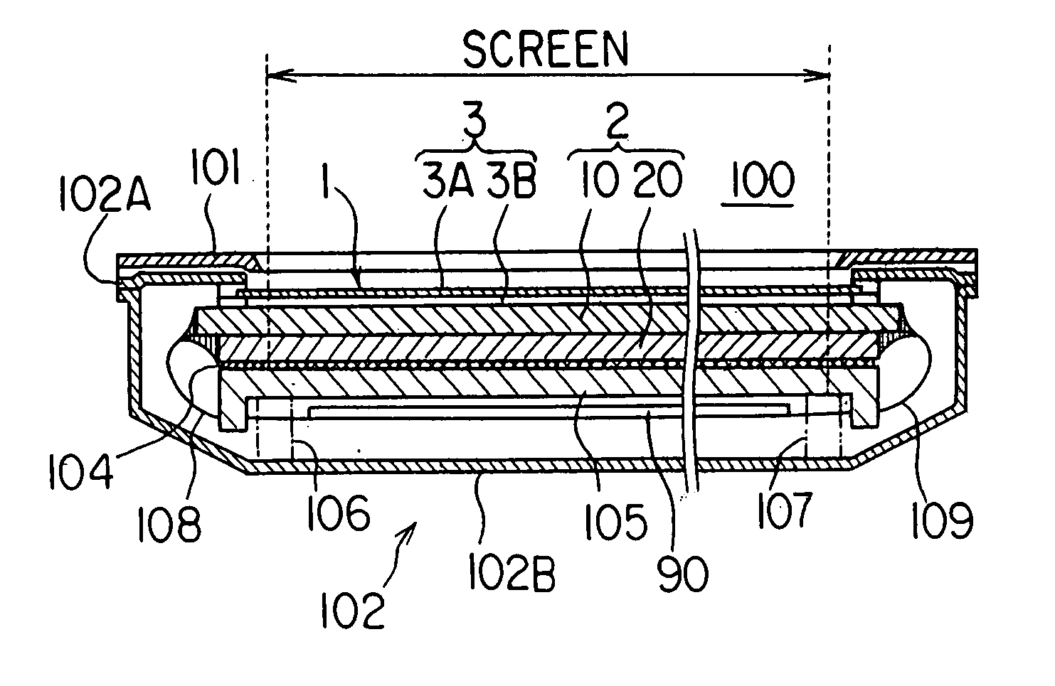
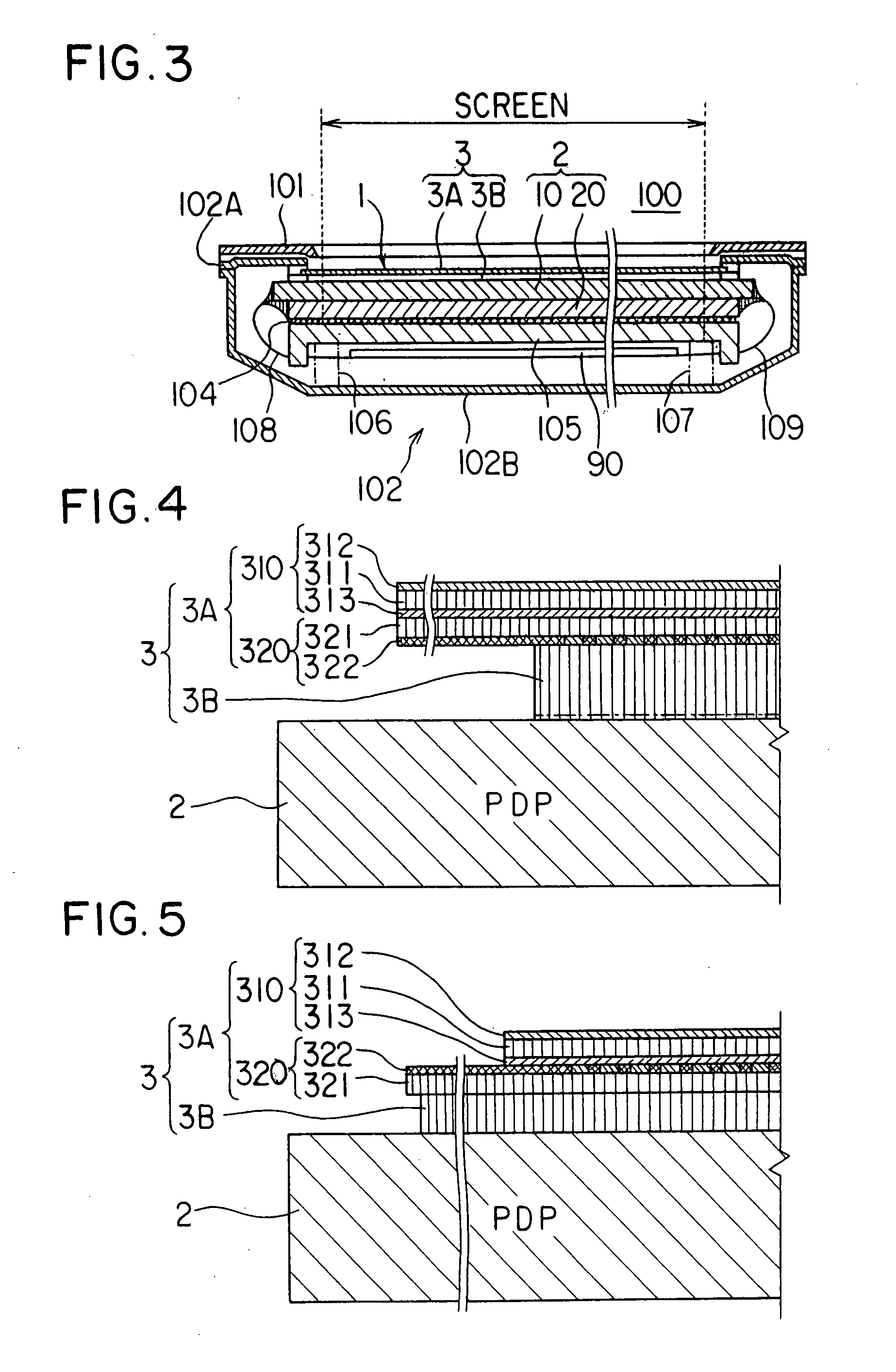
[0077] Scratch resistance on the side of the display surface of a display panel module was tested and investigated by pencil hardness testing. In the display panel module, a function film including a base film 311 of 188 μm thickness and a base film 321 of 125 μm thickness is adhered onto the surface via an adhesive layer 3B of 100 μm thickness in the manner described above. According to the test results, no scratch occurred even at the hardness of HB.
example 2
[0078] In the case that the thickness of the base film 311 is 188 μm, the thickness of the base film 321 is 125 μm, and the thickness of the adhesive layer 3B is 250 μm, no scratch occurred even at the hardness of HB.
example 3
[0079] In the case that the thickness of the base film 311 is 250 μm, the thickness of the base film 321 is 125 μm, and the thickness of the adhesive layer 3B is 500 μm, no scratch occurred even at the hardness of HB.
PUM
 Abstract
Description
Claims
Application Information


