

Acoustic wave device and filter
- Summary
- Abstract
- Description
- Claims
- Application Information
AI Technical Summary
Benefits of technology
Problems solved by technology
Method used
Image

Examples
first embodiment
[0030]FIG. 3 is a cross-sectional view of an acoustic wave device in accordance with a first embodiment of the present invention. In FIG. 3, those parts that are the same as those shown in the previously described figures are given the same reference numerals. A first dielectric film 22a is formed on the piezoelectric substrate 12 may be made of 30° Y-cut X-propagation lithium niobate (LiNbO3). The first dielectric film 22a may be made of silicon oxide (SiO2) and may be 10 nm thick. The comb-like electrodes 14 and the reflection electrodes 16, which may be made of copper (Cu), are provided on the dielectric film 22a at a thickness of, for example, 170 nm. A second dielectric film 24, which may be made of silicon oxide, is provided at a thickness of, for example, 1050 nm, so as to cover the comb-like electrodes 14 and the reflection electrodes 16. A third electric film 26, which may be aluminum oxide, is provided on the second dielectric film 24 at a thickness of, for example, 2 μm.
[...
second embodiment
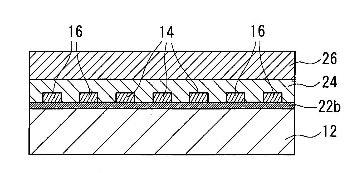
[0037]FIG. 7 is a cross-sectional view of an acoustic wave device in accordance with a second embodiment of the present invention. In FIG. 7, parts that are the same as those shown in the previously described figures are given the same reference numerals. Referring to FIG. 7, a first dielectric film 22b, which may be made of aluminum oxide, is provided on the piezoelectric substrate 12. The other parts of the second embodiment are the same as those of the first embodiment.
[0038]The first dielectric film 22b of aluminum oxide is provided between the piezoelectric substrate 12 and the comb-like electrodes 14 and the reflection electrodes 16. With this structure, it is possible to improve the temperature characteristic of the acoustic wave device, as in the case of the first embodiment.
[0039]The aluminum oxide film of the first dielectric film 22b has a higher resistance to dry or wet etching than the silicon oxide film. Thus, the acoustic wave device of the second embodiment can be fa...
third embodiment
[0045]FIG. 9 is a cross-sectional view of an acoustic wave device in accordance with the third embodiment of the present invention. In FIG. 9, parts that are the same as those shown in the previously described figures are given the same reference numerals. The first dielectric film 22a made of, for example, silicon oxide is provided on the piezoelectric substrate 12 made of, for example, 30° Y-cut X-propagation lithium niobate. The comb-like electrodes 14 and the reflection electrodes 16 made of, for example, copper are provided on the first dielectric film 22a. The second dielectric film 24, which may be made of silicon oxide, is provided so as to cover the comb-like electrodes 14 and the reflection electrodes 16.
[0046]Since the first dielectric film 22a of silicon oxide is provided between the piezoelectric substrate 12a and the comb-like electrodes 14 and the reflection electrodes 16, the third embodiment has an improved temperature characteristic as in the case of the first embo...
PUM
 Abstract
Description
Claims
Application Information