Photoelectric conversion device and imaging device

Inactive Publication Date: 2008-03-13
CANON KK
View PDF32 Cites 67 Cited by
  • Summary
  • Abstract
  • Description
  • Claims
  • Application Information

AI Technical Summary

Benefits of technology

[0008]The present invention has been made to overcome the conventional drawbacks, and has as its object to prevent a

Problems solved by technology

As a result, for example, the number of frames to be photographed per second decreases in a digital still camera, the f

Method used


Image

  • Photoelectric conversion device and imaging device
  • Photoelectric conversion device and imaging device
  • Photoelectric conversion device and imaging device

Examples


first embodiment

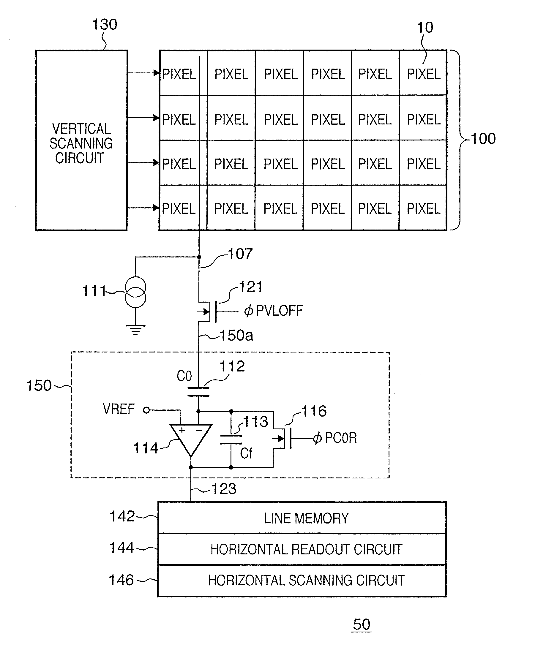
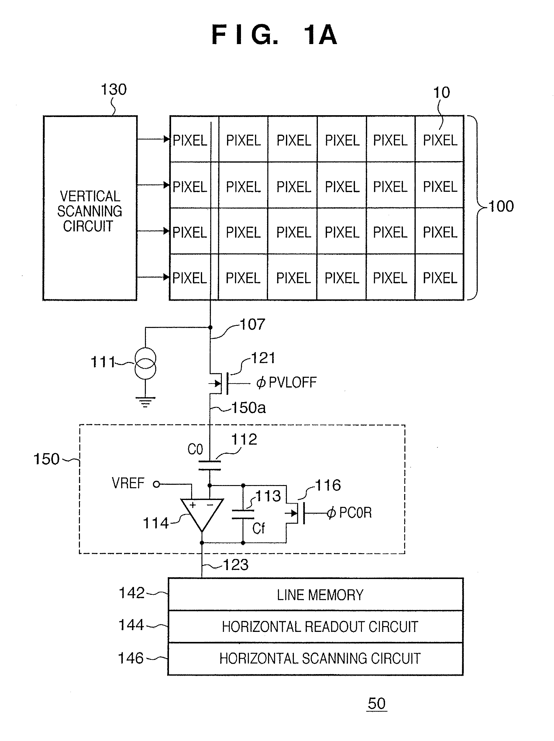
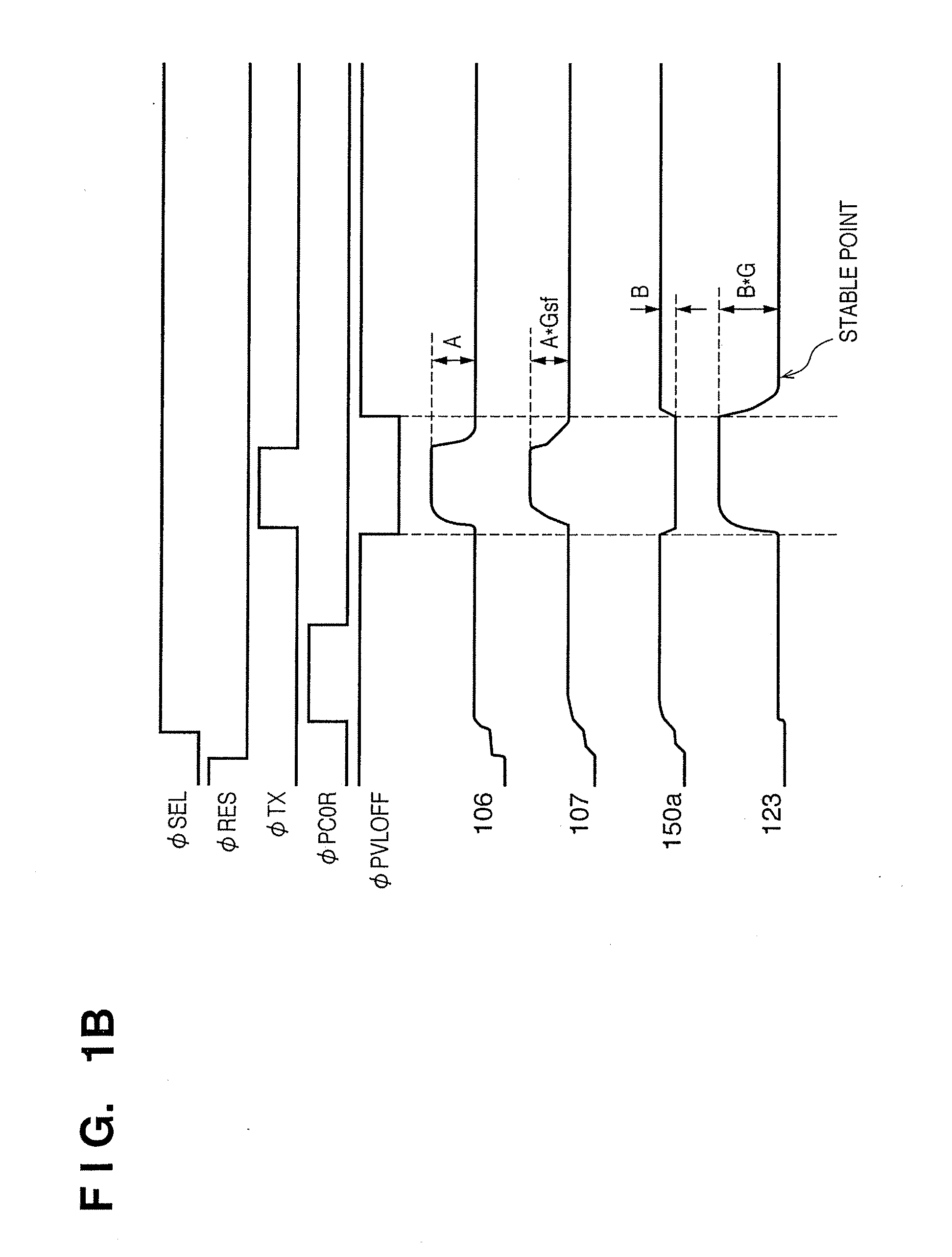
[0026]FIG. 1A is a diagram schematically showing the arrangement of a photoelectric conversion device (solid-state image sensing device) according to the first embodiment of the present invention. A photoelectric conversion device 50 shown in FIG. 1A includes a pixel array 100 in which pixels 10 each shown in FIG. 6 are arrayed in a matrix. A vertical scanning circuit 130 sequentially selects (scans) a plurality of rows which form the pixel array 100. The pixel 10 which belongs to the selected row outputs a signal to a vertical signal line 107 corresponding to the column to which the pixel 10 belongs. FIG. 1A shows only one vertical signal line 107 for the sake of simplicity.

[0027]The pixel 10 shown in FIG. 6 includes a photodiode 101, transfer switch (MOS transistor) 102, reset switch 103, amplification transistor 104, and row selecting transistor 105. The transfer switch 102 transfers a charge generated by the photodiode 101 to a floating diffusion (FD) 106 when a transfer pulse φ...

second embodiment

[0043]FIG. 2A is a diagram schematically showing the arrangement of a photoelectric conversion device (solid-state image sensing device) according to the second embodiment of the present invention. Details which are not particularly referred to here can follow the first embodiment.

[0044]A photoelectric conversion device 60 in this embodiment has the arrangement in which an isolation switch 121 in the first embodiment is replaced with an isolation switch 221. The isolation switch 221 is a parallel circuit of an NMOS transistor 221n and a PMOS transistor 221p having the same size. The gate of the NMOS transistor 221n receives an isolation signal φPVLOFF which is the same as that in the first embodiment, and the gate of the PMOS transistor 221p receives an inverted isolation signal / φPVLOFF serving as the inverted signal of the isolation signal φPVLOFF. With such arrangement, the isolation signal φPVLOFF and the inverted isolation signal / φPVLOFF having the opposite logical levels can ...

third embodiment

[0046]FIG. 3A is a diagram schematically showing the arrangement of a photoelectric conversion device (solid-state image sensing device) according to the third embodiment of the present invention. Details which are not particularly referred to here can follow the first embodiment.

[0047]A photoelectric conversion device 70 according to this embodiment has the arrangement in which an isolation switch 121 in the first embodiment is replaced with an isolation switch 321. FIG. 3B is a circuit diagram showing the arrangement of the isolation switch 321. In this embodiment, the difference between the ON resistances of an NMOS transistor and a PMOS transistor is considered. Generally, the ON resistance of the PMOS transistor is two to three times that of the NMOS transistor. When using these transistors for a transmission switch, the PMOS transistor advantageously transmits a high potential, and the NMOS transistor advantageously transmits a low potential. Hence, when the NMOS and PMOS tran...


PUM


Abstract

A photoelectric conversion device prevents a pseudo signal caused by the parasitic capacitance of a transfer switch from being input to an amplifier. A photoelectric conversion device (50) includes a pixel (10) which outputs a signal to a signal line (107), an amplifier which amplifies the signal supplied via the signal line (107), and an isolation switch (121) inserted between a signal line (108) and the input node of the amplifier. The pixel (10) includes a photodiode, a floating diffusion (FD), a transfer switch which transfers the charge of the photodiode to the FD, and an amplification transistor which outputs a signal to a signal line (109) in accordance with the potential of the FD. The isolation switch (121) is turned off at least in a period when a transfer pulse for controlling the transfer switch of the pixel (10) transits.

Description

BACKGROUND OF THE INVENTION[0001]1. Field of the Invention[0002]The present invention relates to a photoelectric conversion device and an imaging device including it.[0003]2. Description of the Related Art[0004]FIG. 7 is a circuit diagram schematically showing the arrangement of a photoelectric conversion device. A photoelectric conversion device 200 shown in FIG. 7 includes a pixel 10 which outputs a signal to a vertical signal line 107, and an amplifier 11 which amplifies a signal supplied via the vertical signal line 107.[0005]The pixel 10 includes a photodiode 101, transfer switch 102, reset switch 103, amplification transistor 104, and row selecting transistor 105. The transfer switch 102 transfers a charge generated by the photodiode 101 to a floating diffusion (FD) 106 when a transfer pulse φTX is enabled. The amplification transistor 104 constitutes a source-follower circuit with a constant current load 111 connected to the vertical signal line 107, and outputs a signal to t...

Claims


Application Information

Patent Timeline
IPC IPC(8): H04N3/14H01L27/146H01L31/10H04N5/335H04N5/357H04N5/374H04N5/378
CPCH04N3/1575H04N3/1512H04N25/616H04N25/76H04N25/75
Inventor OGURA, MASANORIKOIZUMI, TORUFUJIMURA, MASARU
Owner CANON KK
Why Eureka
Try Eureka