

Electrostatic chuck device
a technology of electrostatic chuck and chuck body, which is applied in the manufacture of semiconductor/solid-state devices, basic electric elements, electric devices, etc., can solve the problems of preventing a uniform plasma process on the plate-like sample, and it is not possible to effectively prevent current from flowing from the peripheral portion, etc., to achieve excellent action and responsiveness of electrostatic adsorption for
- Summary
- Abstract
- Description
- Claims
- Application Information
AI Technical Summary
Benefits of technology
Problems solved by technology
Method used
Image

Examples
first embodiment
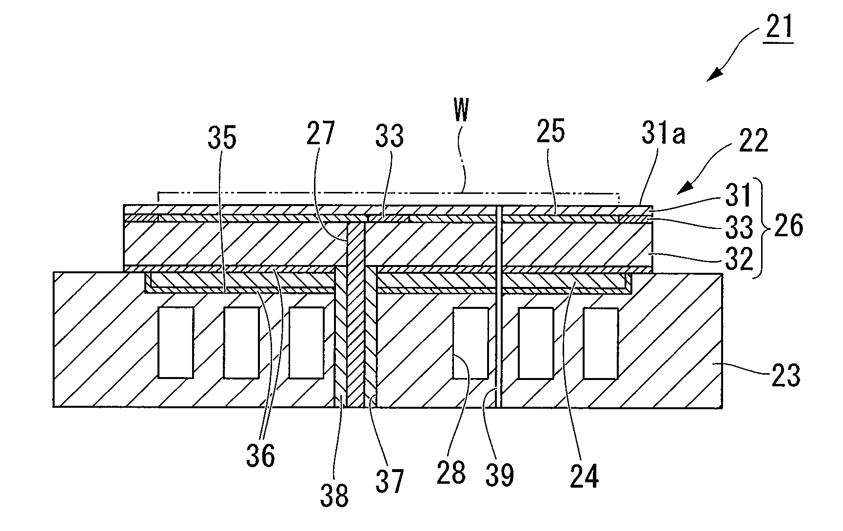
[0036]FIG. 1 is a cross-sectional view illustrating a unipolar electrostatic chuck device 21 according to a first embodiment of the invention. The electrostatic chuck device 21 includes an electrostatic chuck section 22, a metal base section 23, and a dielectric plate 24.
[0037] The electrostatic chuck section 22 includes a disc-like substrate 26, the top surface (one main surface) of which serves as a mounting surface for mounting a plate-like sample W and in which an electrostatic-adsorption inner electrode 25 is built, and a power supply terminal 27 for applying a DC voltage to the electrostatic-adsorption inner electrode 25.
[0038] The substrate 26 roughly includes a disc-like mounting plate 31 of which the top surface 31a (one main surface) serves as the mounting surface for mounting a plate-like sample W such as a semiconductor wafer, a metal wafer, and a glass plate, a disc-like support plate 32 disposed opposite the bottom surface (the other main surface) of the mounting pla...
second embodiment
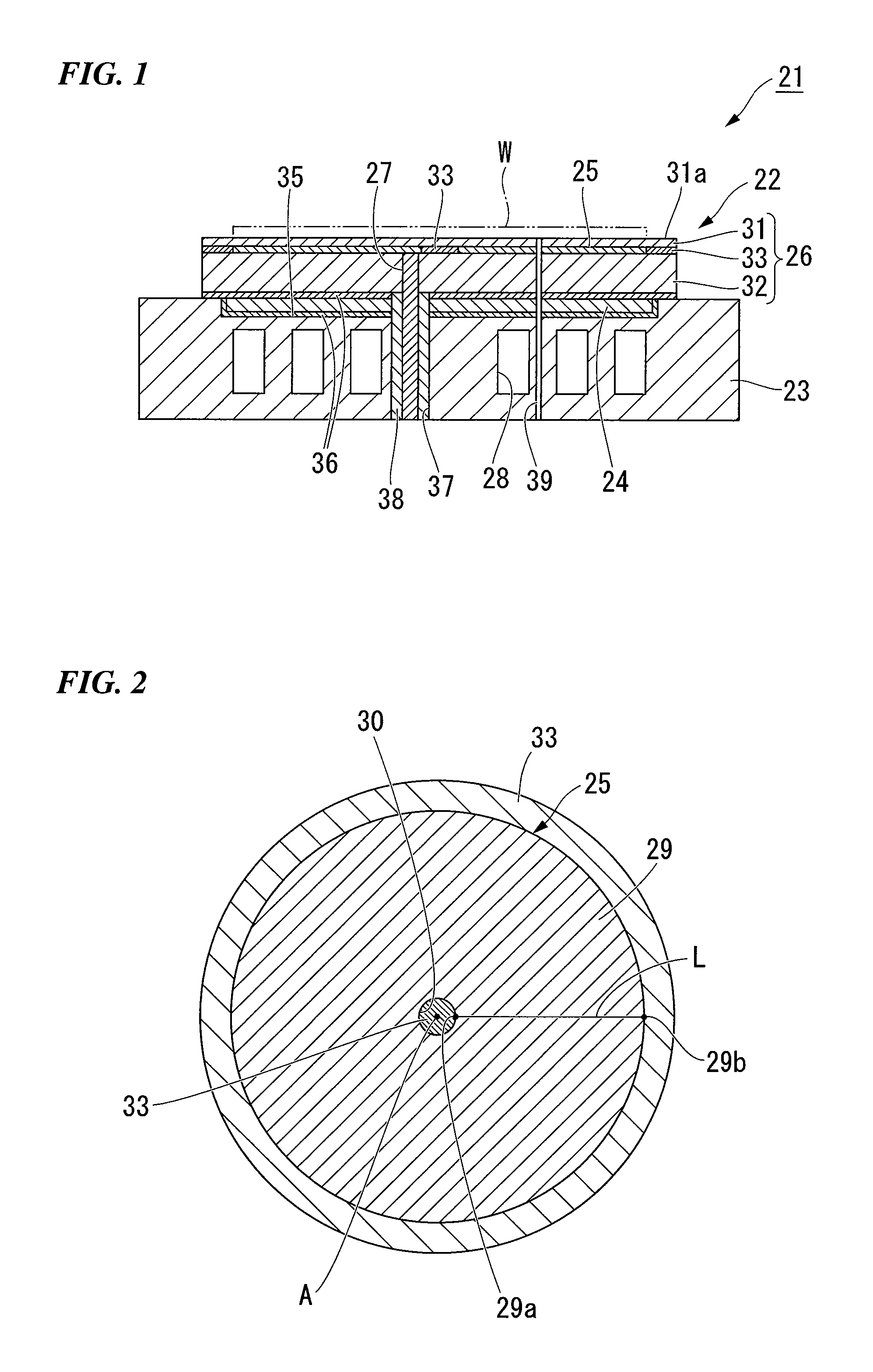
[0097]FIG. 3 is a sectional view illustrating a state where an electrostatic-adsorption inner electrode 41 of a unipolar electrostatic chuck device according to a second embodiment of the invention is formed on the support plate 32 of the substrate 26. The electrostatic-adsorption inner electrode 41 according to this embodiment is different from the electrostatic-adsorption inner electrode 25 according to the first embodiment, in that one electrode portion includes three ring-shaped electrodes 42 to 44 arranged concentrically about the center axis A of the substrate and having different diameters and a plurality of conductive connection portions 45 (eight in FIG. 3) electrically connecting the ring-shaped electrodes 42 to 44 to each other.
[0098] Among distances between two points in the electrode portion, a resistance value of the shortest distance L between a point 42a closest to the center axis A of the substrate and a point most distant from the center axis A, that is, a point 4...
third embodiment
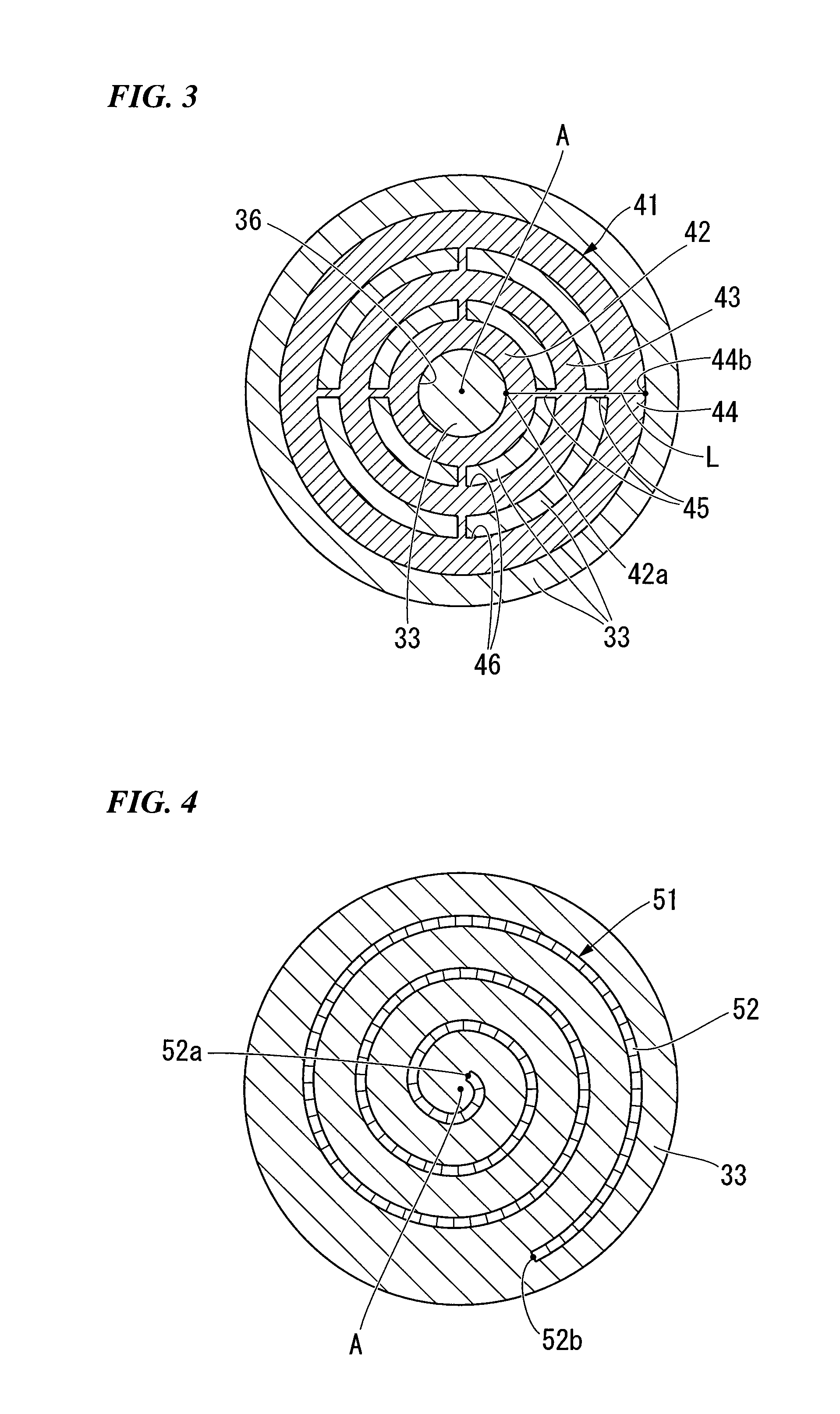
[0101]FIG. 4 is a sectional view illustrating a state where an electrostatic-adsorption inner electrode 51 of a unipolar electrostatic chuck device according to a third embodiment of the invention is formed on the support plate 32 of the substrate 26. The electrostatic-adsorption inner electrode 51 is different from the electrostatic-adsorption inner electrode 25 according to the first embodiment, in that one electrode portion includes one spiral electrode 52 extending in a spiral shape from the vicinity of the center axis A of the substrate to the peripheral edge.
[0102] Among distances between two points in the spiral electrode 52, a resistance value of a distance in the length direction of the spiral electrode 52 between a point 52a closest to the center axis A of the substrate and a point most distant from the center axis A, that is, a point closest to the peripheral edge of the substrate, is in the range of 102 and 1010Ω.
[0103] In the electrostatic-adsorption inner electrode 5...
PUM
 Abstract
Description
Claims
Application Information