

Mounting structure
a technology of mounting structure and mounting plate, which is applied in the direction of electrical apparatus construction details, sustainable manufacturing/processing, and final product manufacturing, etc., can solve the problems of low connection strength at the interface between the solder and the member to be connected, sometimes hindering the connection, and not being able to sink
- Summary
- Abstract
- Description
- Claims
- Application Information
AI Technical Summary
Benefits of technology
Problems solved by technology
Method used
Image

Examples
embodiment 1
[0032]A full grid BGA which is a low heat resistant component (the heat resistant temperature: 220° C., the component size: 23 mm×23 mm, the bump pitch: 1.0 mm, the number of bumps: 484 (22 rows×22 columns), the bump composition: Sn-9Zn) is mounted on a substrate on which a Sn-9Zn solder paste (the supply thickness: 0.15 mm, the supply diameter: 0.5 mm) has been printed, and then reflow soldering is performed so that the peak temperature of the bumps in the center of the component becomes 220° C.
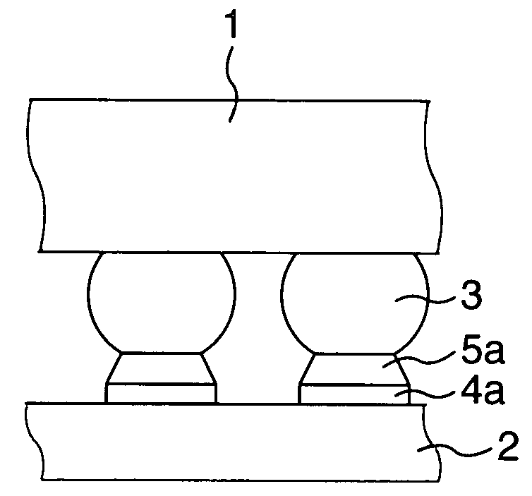
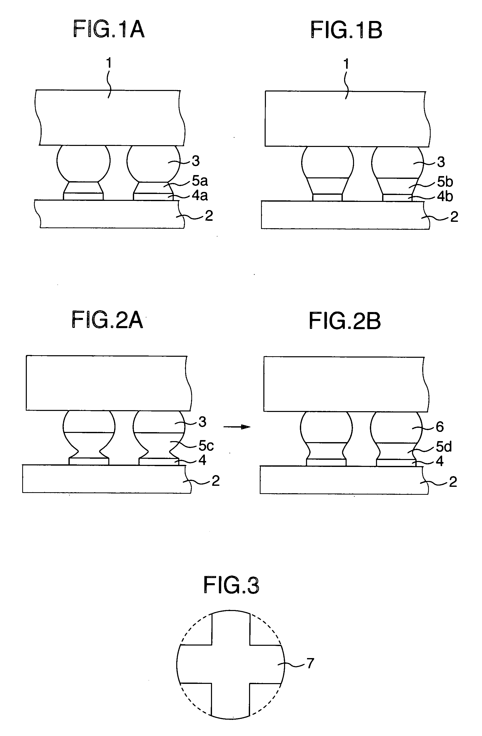
[0033]The following two kinds of substrates are used for the connection. In substrate B, the five columns on an outer side (340 bumps) are set as an outer peripheral portion, and the land size in this portion is made smaller than that in a central portion.
[0034]Therefore, the remaining portion, that is, a portion consisting of the 12 rows×12 columns (144 bumps) is called the central portion.
[0035]For the respective substrate samples, one BGA is connected to each substrate, and 100 substrates...
embodiment 2
[0040]The full grid BGA which is a low heat resistant component (the heat resistant temperature: 220° C., the component size: 23 mm×23 mm, the bump pitch: 1.0 mm, the number of bumps: 484 (22 rows×22 columns), the bump composition: Sn-9Zn) is mounted on the substrate on which the Sn-9Zn solder paste (the supply thickness: 0.15 mm, the supply diameter: 0.5 mm) has been printed, and then the reflow soldering is performed so that the peak temperature of the bumps in the center of the component becomes 220° C.
[0041]The following substrate, and components A and B are used for the connection.
(Substrate)
Land size in central portion (diameter): 0.5 mm
Land size in outer peripheral portion (diameter): 0.5 mm
(Component A)
[0042]No treatment is applied to the BGA.
(Component B)
[0043]The five columns on an outer side of the BGA (340 bumps) are set as an outer peripheral portion, and a part of each bump surface in this portion is coated with a solder resist.
[0044]At this time, the solder resist is ...
embodiment 3
[0050]The full grid BGA which is a low heat resistant component (the heat resistant temperature: 220° C., the component size: 23 mm×23 mm, the bump pitch: 1.0 mm, the number of bumps: 484 (22 rows×22 columns), the bump composition: Sn-9Zn) is mounted on the substrate on which the Sn-9Zn solder paste (the supply thickness: 0.15 mm, the supply diameter: 0.5 mm) has been printed, and then the reflow soldering is performed so that the peak temperature of the bumps in the center of the component becomes 220° C.
[0051]The following two kinds of substrates are used for the connection. In substrate B, the five columns on the outer side (340 bumps) are set as an outer peripheral portion, and each substrate side land shape 7 in this portion is formed so that an outer peripheral length becomes about 3.8 times as large as the land size by providing notched portions at four spots in its circular shape with a diameter of 0.5 mm as shown in FIG. 3.
[0052]Meanwhile, the remaining portion, that is, th...
PUM
 Abstract
Description
Claims
Application Information