NAND flash memory device with ecc protected reserved area for non-volatile storage of redundancy data

a technology of non-volatile storage and flash memory, applied in the field of memory devices, can solve the problems of reducing the yield of the fabrication process, affecting the operation life of the device, so as to reduce the silicon area requirement of the non-volatile memory device, and enhance the fabrication yield. the effect of the device's operating life characteristics

Inactive Publication Date: 2008-03-13
STMICROELECTRONICS SRL +1
View PDF3 Cites 59 Cited by
  • Summary
  • Abstract
  • Description
  • Claims
  • Application Information

AI Technical Summary

Benefits of technology

[0013] In view of the foregoing background, an object of the invention is to reduce silicon area requirement of a non-volatile memory device while achieving enhanced fabrication yields without significantly compromising the operating life characteristics of the device.

Problems solved by technology

The unpredictable though statistically inevitable presence of failed array elements also in such a reserved area of the memory array would likely corrupt the basic redundancy information as established during the test-on wafer (EWS) phase of the fabrication process.
This may increase the number of rejects, and lower the yield of the fabrication process.

Method used


Image

  • NAND flash memory device with ecc protected reserved area for non-volatile storage of redundancy data
  • NAND flash memory device with ecc protected reserved area for non-volatile storage of redundancy data
  • NAND flash memory device with ecc protected reserved area for non-volatile storage of redundancy data

Examples


Embodiment Construction

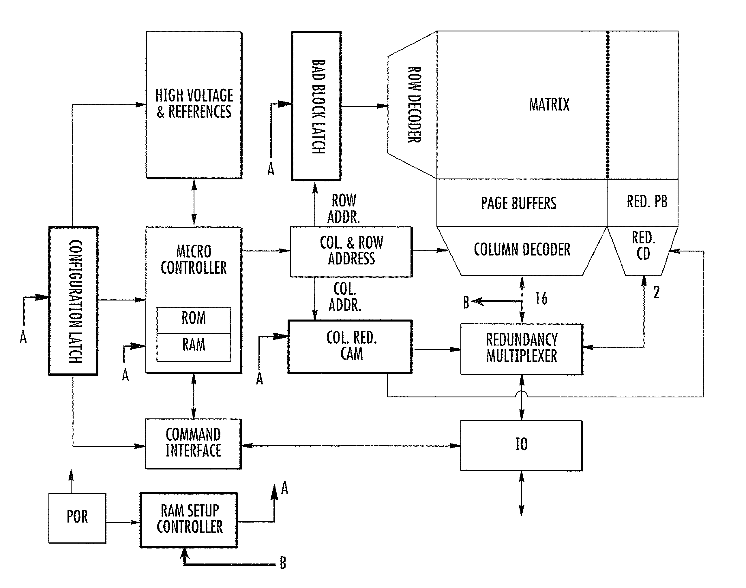
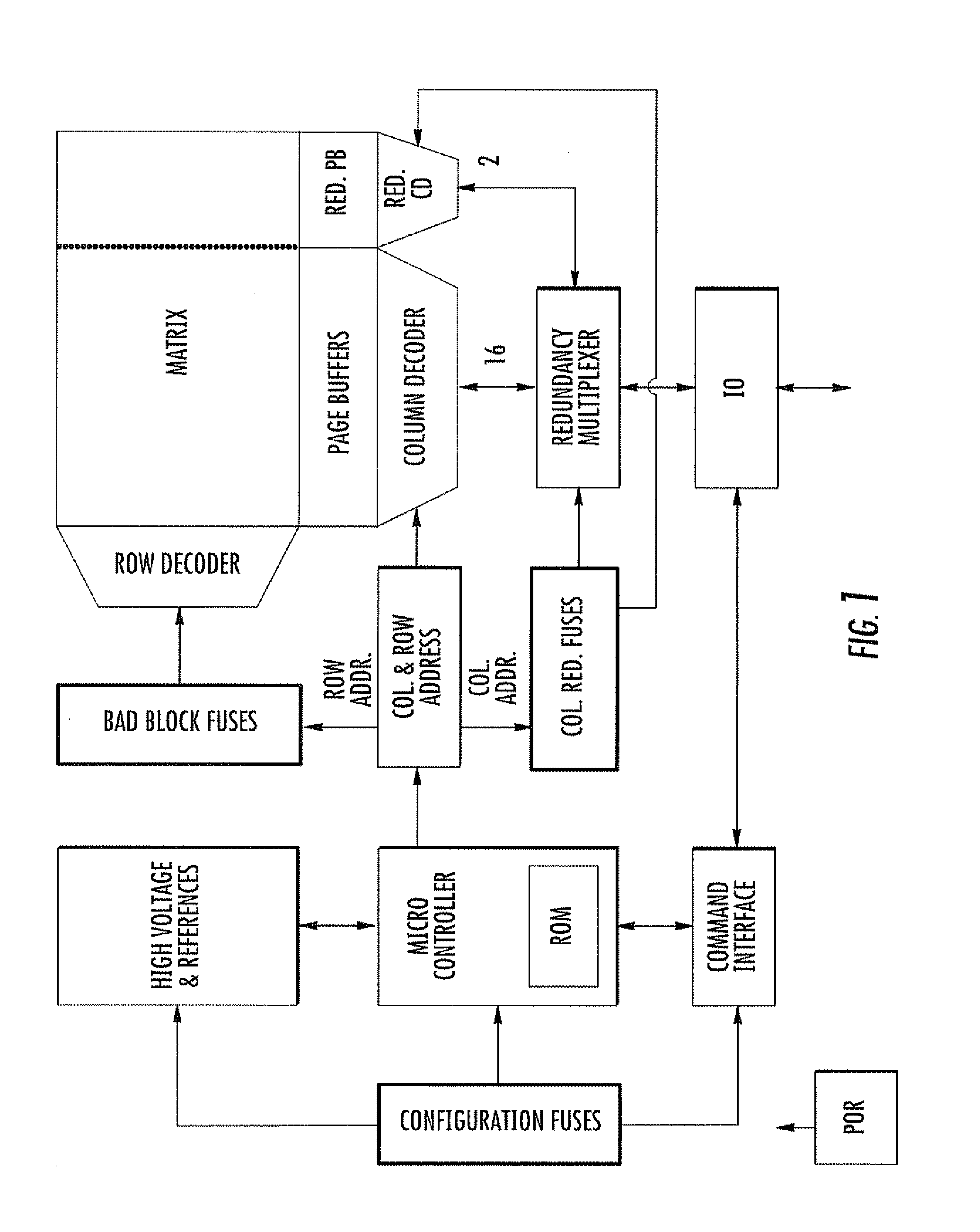
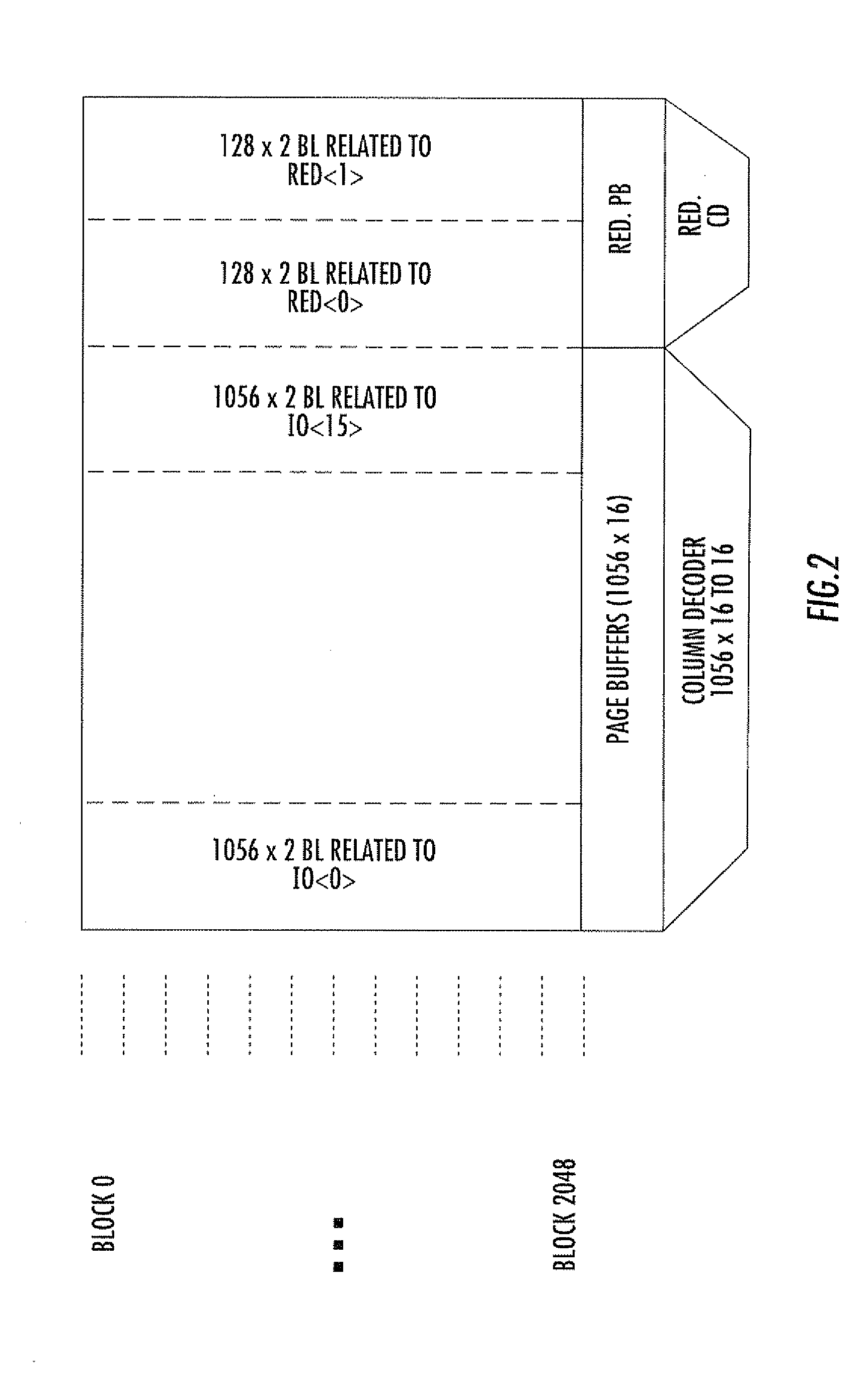
[0023] As graphically represented in FIG. 3, a reserved area RA (identified by the darkened field) that will not be addressable by the user of the EWS-tested, trimmed, repaired and finished memory device is part of the addressable area of the memory cell array. The reserved area RA may retain the same organization graphically defined in FIG. 2.

[0024] In FIG. 3, the dark dots indicate failed cells that cannot be utilized (as identified during the test-on wafer of the device), and the solid vertical lines represent failed bit lines of the array (as also identified during the test-on wafer phase). The basic redundancy data on the failed array elements identified during the EWS testing are written, during the EWS phase itself, in the reserved area RA of the addressable area of the memory cell array. This is identified by the darkened array area in FIG. 3.

[0025] The writing of the basic redundancy data in the reserved area is made with an ECC data writing technique according to a certa...


PUM


Abstract

Basic redundancy information is non-volatily stored in a reserved area of an addressable area of a memory array, and is copied to volatile storage therein at every power-on of the memory device. The unpredictable though statistically inevitable presence of failed array elements in such a reserved area of the memory array corrupts the basic redundancy information established during the test-on wafer (EWS) phase of the fabrication process. This increases the number of rejects, and lowers the yield of the fabrication process. This problem is addressed by writing the basic redundancy data in the reserved area of the array with an ECC technique using a certain error correction code. The error correction code may be chosen among majority codes 3, 5, 7, 15 and the like, or the Hamming code for 1, 2, 3 or more errors, as a function of the fail probability of a memory cell as determined by the EWS phase during fabrication.

Description

FIELD OF THE INVENTION [0001] The present invention relates to memory devices and, more particularly, to a NAND flash memory device with an area efficient redundancy architecture. BACKGROUND OF THE INVENTION [0002] In NAND type memory devices, device specific self-configuration data and redundancy data of identified failed elements of the array of memory cells and substitute elements addresses in the redundant resource area of the array are commonly stored in a non-volatile manner using dedicated fuse arrays. Fuse arrays are permanently set during the testing on wafer (EWS) phase of the devices in the fabrication process. [0003]FIG. 1 is a simplified high level block diagram of a common NAND flash memory device in which the fuse arrays containing the basic data of redundancy and self-configuration implementation at every power-on of the device are highlighted by outlining the relative blocks with a thicker line. These blocks include the CONFIGURATION FUSES block for setting importan...

Claims


Application Information

Patent Timeline
Patent Type & Authority Applications(United States)
IPC IPC(8): G11C29/04
CPCG06F11/1068G11C2029/0411G11C29/82G11C29/24
Inventor MICHELONI, RINORAVASIO, ROBERTOMARELLI, ALESSIA
Owner STMICROELECTRONICS SRL
Why Eureka
Try Eureka